

Award
There are three categories of awards for authors who presented papers at the SSDM:
the SSDM Award, the SSDM Paper Award, and the SSDM Young Researcher Award.
SSDM Award
The SSDM Award was established to recognize outstanding contributions to academic or industrial development in the field of solid state devices and materials. Papers to be nominated for the 2014 SSDM Award should be among those that have been presented between the 1st SSD conference in 1969 and the 40th SSDM conference in 2008. The SSDM Award will ultimately be decided by the SSDM Organizing Committee after a recommendation is made by the SSDM Award Nomination Committee.
-
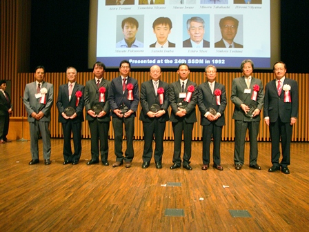
Presented at the 24th International Conference on Solid State Devices and Materials (1992), Tsukuba.High Speed 0.1µm CMOS Devices Operating at Room TemperatureA.Toriumi, T. Mizuno, M. Iwase, M. Takahashi, H. Niiyama, M. Fukumoto, S. Inaba, I. Mori, and M. Yoshimi
(ULSI Research Center, Toshiba Corporation)
This paper succeeded in demonstrating the promising features of room-temperature-operation 0.1-µm CMOS devices as the main stream technology in the era of sub-0.1-µm VLSI circuits as early as in 1992. Important to note is that such features were demonstrated without introducing any esoteric technologies, but using standard technologies of most advanced features at the time. The authors fabricated both NMOS and PMOS transistors having 0.1-µm gate length employing electron beam lithography for gate patterning and rapid thermal annealing for source/drain formation with titanium salicide processing. The authors demonstrated for the first time that the very high-speed switching operation of 0.1-µm CMOS integrated circuits at room temperature by fabricating ring oscillators, and that the feasibility of the 0.1-µm device technology by studying the current-voltage characteristics of fabricated NMOS and PMOS transistors.
When we look back to the years from the late 80’s to the early 90’s, the 0.25-µm CMOS technology was being brought into production. However, the challenges for 0.1-µm CMOS or beyond were quite in controversy. People believed that introduction of some new innovative technologies were inevitable. To cite some, low temperature (77K) CMOS, epi-channel FETs, FinFETs, BiCMOS were in hot dispute. After the successful demonstration of 0.1-µm CMOS integrated circuits operation at room temperature using non-esoteric technologies by the authors, however, the world trend for the exploration for the next generation VLSI devices were refocused to the direction shown by the work.
The role played by this paper at the time of 1992 is really significant in that it showed the right direction of for CMOS technology development that have persisted right up to the current 20-nm generation that we have been witnessing.
-
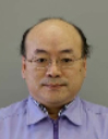
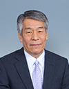
Akira Toriumi
The University of TokyoAkira Toriumi can be reached by e-mail at toriumi@material.t.u-tokyo.ac.jp. He is a professor of Materials Engineering at The University of Tokyo, Japan. He received the B.S. degree in physics, the M.S. and Ph.D. degrees in applied physics from The University of Tokyo. He joined Research and Development Center of Toshiba Corporation in 1983, when he touched Si for the first time. Then he moved to The University of Tokyo in 2000. His current research interests include materials science and device physics for scaled CMOS not only in Si but also in Ge and other new materials. Through his professional carriers, he has mainly studied gate stack technology in field-effect devices of various materials. He was in charge of high-k gate stack group in MIRAI Project in Japan from 2001 to 2007. He is a fellow of the Japan Society of Applied Physics.
-
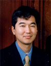
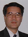
Tomohisa Mizuno
Kanagawa UniversityTomohisa Mizuno was born in, Gifu, Japan, on May 12, 1955. He received the B.S. degree in physics, the M.S. degree in astrophysics, and the Ph.D. degree in applied physics from Nagoya University, Nagoya, Japan, in 1979, 1981, and 1991, respectively.
In 1982, he joined the Semiconductor Device Engineering Lab., Toshiba Corp., Kawasaki, Japan, where he was engaged in the research and development of 1M/16M bit CMOS-DRAMs, SiN LDD spacer, vertical MOSFETs with dual gates, and shallow-junction-well transistors (SJET). Since 1990, he has been engaged in the research of scaled CMOS, and device physics of statistical performance variations due to dopant density fluctuations and carrier’s velocity overshoot of CMOS devices including SOI structures in Toshiba R&D center. In April 2004, he moved to Kanagawa University, where he is a professor in faculty of science. Currently, he is now working on low-dimensional Si structures and source heterojunction for future high-speed CMOS devices. -
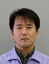
Masao Iwase
Toshiba Corporation
Semiconductor & Storage Products CompanyMasao Iwase Masao Iwase joined the Research and Development Center, Toshiba Corporation, Kawasaki, Japan, in 1982, where he was engaged in the research of electron beam lithography and in the development of deep-submicrometer CMOS technologies. He was also involved in the development of Micro-ID technologies until 2002. For recent years, he was long engaged in the development of advanced flash memory technologies. He currently works at the Advanced Memory Development Center, Semiconductor & Storage Products Company, Toshiba Corporation.
-
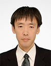
Minoru Takahashi
Toshiba Corporation
Semiconductor & Storage Products CompanyMinoru Takahashi was born in Akita, Japan, in 1961. He graduated from the Technical High School of Yokote, Akita, Japan, in 1980. He Joined R&D Center, Toshiba Corporation, Kawasaki Japan in 1980. He was engaged in the research of miniaturization of CMOS devices until 1993. After that, he was engaged in development of CMOS Logic LSIs until 2010. Currently, he is engaged in the development of advanced CMOS image sensor devices at Toshiba Oita-fab.
-
Hiromi Niiyama
Toshiba Corporation
Semiconductor & Storage Products CompanyHiromi Niiyama was born in Hokkaido Japan, in 1966. He graduated from the High School of Mori, Hokkaido, Japan, in 1985. He Joined Toshiba ULSI Research Laboratories, Kawasaki, Japan in 1985. From 1991 to 1998, he was engaged in the development of Electron Beam Direct Writing (EBDW) technology. He was also engaged in the development of Electron-Beam / Deep-Ultraviolet Interlevel Mix-and-Match Lithography technology for CMOS applications. He is currently working as a Lithography engineer for flash memory fabrication at Toshiba Yokkaichi-fab.
-
Masato Fukumoto
Toshiba Corporation
Semiconductor & Storage Products CompanyMasato Fukumoto was born in Kagoshima Japan in 1967.
He joined the Toshiba ULSI Research Institute in 1985.
He was engaged in research on miniaturization of CMOS until 1993, where he was responsible for the RIE of miniaturization process.
1999 to 2009, he was engaged in CMOS Logic LSI Process development, where he was responsible for the Hot Process.
He is now engaged in the Process & Manufacturing Engineering Dept at Toshiba Oita factory. -
Satoshi Inaba
Toshiba Electronics Korea CorporationSatoshi Inaba received the B.S. degree in applied physics, the M.S. degree in physics and the Ph.D. degree in applied physics all from Waseda University, Tokyo, Japan, in 1988, 1990 and 2006, respectively.
He joined the ULSI Research Center, Toshiba Corporation, Kawasaki, Japan in 1990, where he was engaged in R&D for 0.1 mm gate length CMOS and related device technology. From 1998 to 2000, he was with IBM-Infineon-TOSHIBA 256M bit DRAM Development Alliance, Hopewell Junction, NY. In 2000, he joined advanced CMOS technology department, Toshiba Corporation Semiconductor Company, where he was engaged in R&D of high performance and low power sub-50 nm CMOS devices including FinFETs. He was also with MIRAI-SELETE project, NSI Robust Transistor Design Program, Semiconductor Leading Edge Technologies (SELETE), Tsukuba, Japan from 2006 to 2011. He joined Toshiba Electronics Korea Corporation, Seoul, South Korea in 2012. Since then, he has been engaged in memory device development for STT-RAM.
Dr. Inaba has served on the committees/sub-committees of several technical conferences, including SSDM (2002- 2004), IEDM (2003-2004), and Symp. on VLSI Technology (2008-2014). He is currently in charge of the technical program chair of 2015 Symp. on VLSI Tech.
Dr. Inaba is a member of the Physical Society of Japan, the Japan Society of Applied Physics and a senior member of the IEEE Electron Device Society. -
Ichiro Mori
EUVL Infrastructure Development Center, Inc. (EIDEC)Ichiro Mori has been President of EUVL Infrastructure Development Center (EIDEC) since April 2014. From 2011 until 2013 he served as the Company’s director of technology and from 2004 to 2010 he was director and general manager of Semiconductor Leading Edge Technologies (Selete). He had the responsibility for the technical leadership and execution of development program activities on EUV lithography and EUV-related mask technology during this period. Prior to joining these research consortia, he managed research and development of advanced lithography technologies in Toshiba for 12 years from 1992. He started his Semiconductor career with Toshiba, in 1977, where his responsibility covered next generation lithography developments including electron image projection, proximity X-ray lithography and e-beam direct writing. He received his M.S. degree in physics from Waseda University, Japan.
-
Makoto Yoshimi
aBeam Technologies Japan, Inc.Makoto Yoshimi received the B.S. and the M.S. degrees in physical engineering, the University of Tokyo, Japan, in 1975 and 1977, respectively. In 1977, he joined the Research and Development Center, Toshiba Corporation, Kawasaki, Japan, where he started his career with the development of electron-beam exposure lithography system. After that, he was engaged in the development of SOI technologies, including 3D-integration by electron-beam recrystallization technologies, and study on fully-depleted SOI devices. In 1991, he received the Ph.D degree from the University of Tokyo by his work on SOI technologies. In the 90’s, he was engaged in CMOS device technologies, including 0.1µm-CMOS devices, low-voltage low-power SOI CMOS technologies, lateral-bipolar SOI BiCMOS devices, and so on. In 2003, he joined Soitec Asia (currently, Soitec Japan), Inc., where he served as Technology Director and Vice President, contributing to practical applications of bonded SOI wafers to MPUs, RF devices, power devices, MEMS, and so on. Currently, he is serving as CEO of aBeam Technology Japan, Inc., where he is working on simulation technologies on electron-beam technologies. He has published more than 70 technical papers and 100 patents.
 Call for 2014 SSDM Award Nomination
History of the SSDM Award is here
SSDM Paper Award
The SSDM Paper Award will be given for the best paper presented at the conference last year. The award-papers will be decided by the program committee.
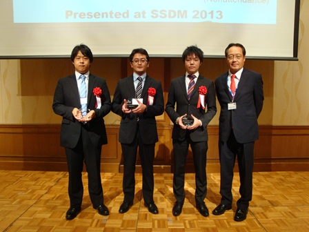
SSDM Paper Award 2014 will be awarded to the best paper presented at SSDM2013.
-
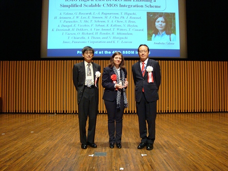
Presentation No.B-1-2 [Area 1]Thermal and Plasma Treatments for Improved (Sub-)1nm EOT Planar and FinFET-based RMG High-k Last Devices and Enabling a Simplified Scalable CMOS Integration SchemeA. Veloso1, G. Boccardi1, L.Å. Ragnarsson1, Y. Higuchi2, H. Arimura1,3, J.W. Lee1,3, E. Simoen1, M.J. Cho1, Ph.J. Roussel1, V. Paraschiv1, X. Shi1, T. Schram1, S.A. Chew1, S. Brus1, A. Dangol1, E. Vecchio1, F. Sebaai1, K. Kellens1, N. Heylen1, K. Devriendt1, H. Dekkers1, A. Van Ammel1, T. Witters1, T. Conard1, I. Vaesen1, O. Richard1, H. Bender1, R. Athimulam1, T. Chiarella1, A. Thean1 and N. Horiguchi1
( 1 Imec, 2 Panasonic and 3 K. U. Leuven)
 History of the SSDM Paper Award is here
SSDM Young Researcher Award
The SSDM Young Researcher Award will be given for outstanding young researchers presented at the conference last year. The award recipients will be decided by the program committee.
*Young researchers who are eligible for the award should be 30 years old or younger at the end of the year of the corresponding conference.
SSDM Young Researcher Award 2014 will be awarded to outstanding papers authored by young researchers and presented at SSDM2013.
-
Presentation No.D-3-2 [Area 3]Channel Length Scaling Limits of III-V Channel MOSFETs Governed by Source-Drain Direct TunnelingS. Koba1, M. Ohmori1, Y. Maegawa1, H. Tsuchiya1,2, Y. Kamakura2,3, N. Mori2,3 and M. Ogawa1
( 1 Kobe Univ., 2 JST-CREST and 3 Osaka Univ.) -
Presentation No.A-2-4 [Area 4]Excellent Scalability Including Self-Heating Phenomena of Vertical-Channel Field-Effect-Diode (FED) Type Capacitorless One Transistor DRAM CellT. Imamoto1,2 and T. Endoh1,2
( 1 Tohoku Univ. and 2 JST-CREST) -
Presentation No.K-1-3 [Area 7]High Speed Waveguide Integrated Lateral P-I-N Ge on Si Photodiode with very Low Dark CurrentL. Virot1,2,3, L. Vivien1, J.M. Hartmann2, Y. Bogumilowicz2, J.M. Fedeli2, D. Marris Morini1, E. Cassan1, C. Baudot3 and F. Boeuf3
( 1 Institut d'Electronique Fondamentale, 2 CEA-Leti and 3 STMicroelectronics) -
Presentation No.G-1-5 [Area 11]An implantable CMOS device for functional brain imaging under freely moving experiments of ratsM. Haruta, C. Kitsumoto, Y. Sunaga, H. Takehara, T. Noda, K. Sasagawa, T. Tokuda and J. Ohta
(Nara Inst. of Sci. and Tech.) -
Presentation No.F-1-5 [Area 12]Gate Control of Spatial Electron Spin Distribution in Persistent Spin Helix StateY. Kunihashi1, H. Sanada1, H. Gotoh1, K. Onomitsu1, M. Kohda2, J. Nitta2 and T. Sogawa1
( 1 NTT BRL and 2 Tohoku Univ.) -
Presentation No.C-3-3 [Area 13]Transport Properties and Defects at the Intersection of CVD Graphene DomainsY. Ogawa1, K. Kawahara1, M. Miyashita1, M. Tsuji1, K. Komatsu2, K. Tsukagoshi2 and H. Ago1
( 1 Kyushu Univ. and 2 National Inst. for Materials Sci.)
 History of the SSDM Young Researcher Award is here
Call for 2014 SSDM Award Nomination
The recommendation will be in accordance with the following two criteria.
-
1) Originality
The Award-winning selection must be original and must have had a significant theoretical or practical impact in the field of solid state devices and materials.
-
2) Contribution
The author(s) of the Award-winning selection must have played or be playing a pioneering or leading role, with globally outstanding contributions, in the technology area of the nomination.
Candidate and Nominator Eligibility
-
- Candidates Eligible for the Award
All authors who presented papers between the 1st SSD conference in 1969 and the 40th SSDM conference in 2008, excluding the following
1) Authors who have passed away
-
- Eligible Nominators and Endorsers
Anyone, excluding the following
1) The author of the paper to be nominated
2) Present members of the SSDM Award Nomination Committee
Submission Process for SSDM Award nominations
The following is the process for submitting nominations.
- - Before deciding on a candidate for the Award, confirm the eligibility of nominators and candidates once again.
- - Download the Nomination Form.
- - Fill out the Nomination Form and send it to the SSDM Secretariat by the nomination deadline.
If you have any questions, please ask the secretariat by e-mail
Kyodo Tsushin Kaikan 4F, 2-2-5 Toranomon, Minato-ku, Tokyo 105-0001, Japan