


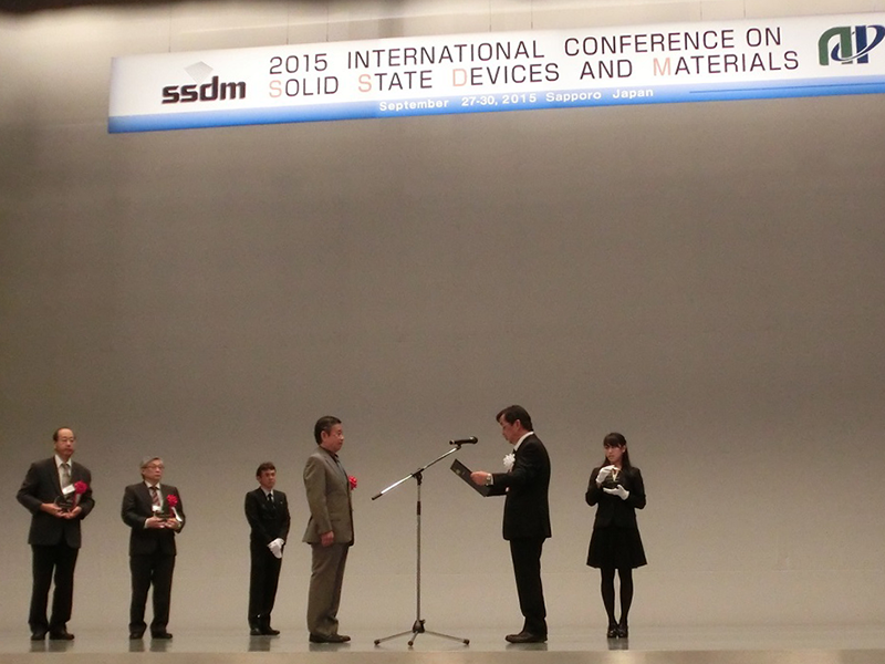
Award
There are three categories of awards for authors who presented papers at the SSDM:
the SSDM Award, the SSDM Paper Award, and the SSDM Young Researcher Award.
SSDM Award
The SSDM Award was established to recognize outstanding contributions to academic or industrial development in the field of solid state devices and materials. Papers to be nominated for the 2015 SSDM Award should be among those that have been presented between the 1st SSD conference in 1969 and the 41st SSDM conference in 2009. The SSDM Award will ultimately be decided by the SSDM Organizing Committee after a recommendation is made by the SSDM Award Nomination Committee.
-
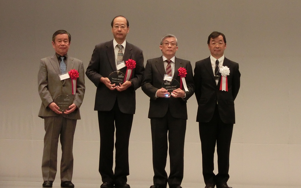
Presented at the 19th International Conference on Solid State Devices and Materials (1987), Tokyo.Highly Reliable Ta2O5/SiO2 Double Dielectric Films on Poly Crystalline SiliconH. Shinriki, Y. Nishioka, and K. Mukai
(Central Research Laboratory, Hitachi, Ltd.)
In this paper, it was demonstrated for the first time that thin Ta2O5/SiO2 double dielectric films formed on polycrystalline silicon can be utilized as a highly reliable insulator for the stacked capacitor of DRAM memory cells; a sufficiently long reliability life of the film with low leakage current was verified under high voltage bias stresses for an equivalent oxide thickness of the Ta2O5/SiO2 film as thin as 4 to 5 nm by experiments.
When we look back to the years from the late 70s to the 80s, the introduction of high-permittivity films and 3D structures to DRAM memory cells was an inevitable technical trend in the DRAM development. SiO2/Si3N4 dielectric films and 3D structures such as trench and stacked capacitors were developed during this period. The role played by this paper at the time of 1987 is greatly significant in that it showed the practical applicability of the stacked high-permittivity dielectric Ta2O5/SiO2 capacitor formed on an n+ polysilicon electrode and confirmed the direction of DRAM development for following generations. In fact, the Ta2O5 stacked capacitors were employed in DRAM products in multiple generations, including 64Mbit DRAM and beyond.
Since this work triggered DRAM development employing stacked-capacitor memory cell structures, the contribution of this paper to semiconductor technology is highly praised.
-
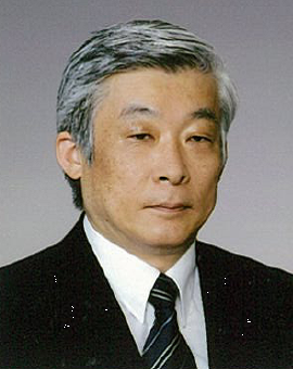
Hiroshi Shinriki
Hiroshi Shinriki received the B.S. and M.S. degree in chemistry from the University of Tokyo. In 1981 he joined Hitachi Ltd., and was engaged in developing plasma CVD for DRAM passivation until 1984. Since then, he was involved in the research of Ta2O5 film and developed CVD-Ta2O5 fabrication techniques including post-annealing processes like UV-O3 for stacked capacitor beyond 64 Mbit DRAMs. In 1995, he moved to the Central Research Laboratory Tokyo Electron Ltd., and had the responsibility for development of multi-chamber cluster tools equipped with CVD, ALD and pre and post treatments for forming Ta2O5, BST, PZT, HfOx, and Al2O3 films and collaborated with several device suppliers for establishing their high-K dielectric processes. In 2004, he moved to ASM japan and engaged in development of advanced ALD tool for high-K dielectric and metals. Currently, he is engaged in consultation for intellectual properties for CVD processes. This paper is the first accepted international conference paper in the research of Ta2O5 for DRAM application.
-
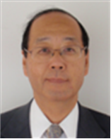
Yasushiro Nishioka
Yasushiro Nishioka received Ph. D. degrees in physics from the University of Tokyo in 1980. After joining the Central Research Laboratory, Hitachi Ltd., in 1981, he researched on high dielectric constant insulators and ultrathin gate insulators for use in VLSIs. He was a visiting scientist with the Department of Electrical Engineering, Yale University, from 1986 to 1988, and studied on influences of fluorine on gate insulator reliability. He moved to the Texas Instruments Tsukuba Research and Development Center as a branch manager of Advanced Materials and Processes in 1991. He has been a professor in the Department of Precision Machinery Engineering, College of Science and Technology, Nihon University, since 2003. His current interests are related to microelectromechanical systems (MEMS) and organic semiconductors.
-
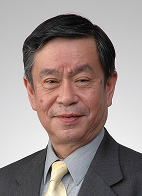
Kiichiro Mukai
Kiichiro Mukai is a free researcher studying “Design of Innovation Fields” based on his carrier of semiconductor technologies development, where he always tried to connect cross-cultural technologies.
Previously, Mukai was Vice President and Executive Officer of Hitachi Kokusai Electric Inc.. He served as General Manager of Semiconductor Equipment Division. Mukai was responsible for Thermal Process Technologies Development of Thin Film Growth including High-k materials, since he joined Hitachi Kokusai in 1996.
Prior to that, Mukai was General manager of Semiconductor Process Technologies , Device Development Center, Hitachi Ltd., from 1991 to 1996. He was responsible for device and process technologies of Logic and Memory, where he was engaged in Ta2O5 capacitor technology for DRAM.
During 1971-1991, Mukai was working for Semiconductor Materials Science and Process Technologies in Central Research Laboratory, Hitachi Ltd.. His research unit introduced new materials in Semiconductor Industry, such as Polyimide, High-K Ta2O5 and Low-k HSG, by means of connecting various knowledge bases outside his unit team. His unit also first developed single wafer type cluster tool in dry etching. Mukai joined Hitachi Ltd. In 1971.
Mukai holds MS degree in Applied Physics from Tokyo Institute of Technology in 1971.
 Call for 2015 SSDM Award Nomination
History of the SSDM Award is here
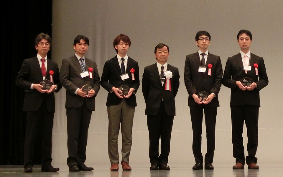
SSDM Paper Award
The SSDM Paper Award will be given for the best paper presented at the conference last year. The award-papers will be decided by the program committee.
SSDM Paper Award 2015 will be awarded to the best paper presented at SSDM2014.
-
Presentation No. F-1-2 [Area 1]Operations of CMOS Inverter and Ring Oscillator Composed of Ultra-Thin Body Poly-Ge p- and n-MISFETs for Stacked Channel 3D-ICY. Kamata1, M. Koike1, E. Kurosawa1, M. Kurosawa2, H. Ota1, O. Nakatsuka2, S. Zaima2, and T. Tezuka1
(1AIST and 2Nagoya Univ.)
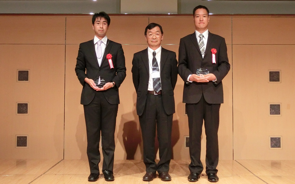
SSDM Young Researcher Award
The SSDM Young Researcher Award will be given for outstanding young researchers presented at the conference last year. The award recipients will be decided by the program committee.
* Young researchers who are eligible for the award should be 30 years old or younger at the end of the year of the corresponding conference.
SSDM Young Researcher Award 2015 will be awarded to outstanding papers authored by young researchers and presented at SSDM2014.
-
Presentation No. J-2-2 [Area 3]Improvement of S-factor method for evaluation of MOS interface state densityW.–L. Cai1,2, M. Takenaka1,2 and S. Takagi1,2
(1Univ. of Tokyo and 2JST-CREST) -
Presentation No. K-1-6 [Area 10]Heat protection circuit with polymer PTC for flexible electronicsT. Yokota1,2, Y. Terakawa1, J. Reeder1,3, M. Kaltenbrunner1,2, T. Ware3, W. Voit3, T. Sekitani2,4 and T. Someya1,2
(1Univ. of Tokyo, 2JST ERATO, 3Univ. of Texas and 4Univ. of Osaka) -
Presentation No. D-1-6 [Area 11]Ultra-High Selective Gas Sensors: novel approaches and future developmentsM. W. G. Hoffmann1,3,5, J. D. Prades3, L. Mayrhofer2, F. Ramirez3,4, T. T. Järvi2, M. Moseler2, A. Waag1,5 and H. Shen1,5
(1Braunschweig Univ. of Technology, 2 Fraunhofer Institute for Mechanics of Materials, 3 Univ. of Barcelona, 4 Catalonia Institute for Energy Research and 5 Laboratory of Nanometrology, Braunschweig Univ. of Technology) -
Presentation No. M-1-4 [Area 12]Excitation of Electric-Field-induced Spin Wave in the Strained Garnet Ferrite Thin Films Using Sub-Picosecond Pulsed WaveM. Adachi, H. Yamaharai, M. Seki, H. Matsui and H. Tabata
(Univ. of Tokyo) -
Presentation No. E-4-4L [Area 14]3.3 kV/1500 A Power Modules for the World's First All-SiC Traction InverterK. Hamada1, S. Hino1,2, N. Miura1, H. Watanabe1,2, S. Nakata1,2, E. Suekawa3, Y. Ebiike3, M. Imaizumi3, I. Umezaki3 and S. Yamakawa1,2
(1Advanced Technology R&D Center, Mitsubishi Electric Corp., 2 R&D Partnership for Future Power Electronics Technology (FUPET) and 3 Power Device Works, Mitsubishi Electric Corp.)
Call for 2015 SSDM Award Nomination
The SSDM Award was established to recognize outstanding contributions to academic or industrial development in the field of solid state devices and materials. Papers to be nominated for the 2015 SSDM Award should be among those that have been presented between the 1st SSD conference in 1969 and the 41th SSDM conference in 2009.
The SSDM Award will ultimately be decided by the SSDM Organizing Committee after a recommendation is made by the SSDM Award Nomination Committee.
The recommendation will be in accordance with the following two criteria.
-
1) Originality
The Award-winning selection must be original and must have had a significant theoretical or practical impact in the field of solid state devices and materials.
-
2) Contribution
The author(s) of the Award-winning selection must have played or be playing a pioneering or leading role, with globally outstanding contributions, in the technology area of the nomination.
Candidate and Nominator Eligibility
-
- Candidates Eligible for the Award
All authors who presented papers between the 1st SSD conference in 1969 and the 41th SSDM conference in 2009, excluding the following
- 1) Authors who have passed away
-
- Eligible Nominators and Endorsers
Anyone, excluding the following
- 1) The author of the paper to be nominated
- 2) Present members of the SSDM Award Nomination Committee
Submission Process for SSDM Award nominations
The following is the process for submitting nominations.
- - Before deciding on a candidate for the Award, confirm the eligibility of nominators and candidates once again.
-
- Download the Nomination Form.
- •SSDM Award Nomination Form [PDF]
- •SSDM Award Nomination Form [MS-Word]
- - Fill out the Nomination Form and send it to the SSDM Secretariat by the nomination deadline.
Nomination deadline: March 9, 2015 closed
If you have any questions, please ask the secretariat by e-mail
Sumitomo-Shoji Kanda-Izumi-cho Bldg., 12F
1-13 Kanda-Izumi-cho, Chiyoda-ku, Tokyo 101-0024
closed on March 27