
Award
There are three categories of awards for authors who presented papers at the SSDM:
the SSDM Award, the SSDM Paper Award, and the SSDM Young Researcher Award.
SSDM Award
The SSDM Award will be will be awarded to researchers who contributed an outstanding paper at past SSDM. The Award Committee selects this award.
-
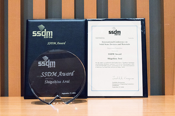
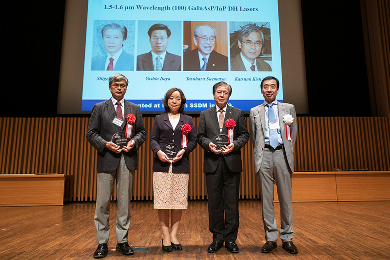
Presented at the 11th International Conference on Solid State Devices and Materials (1979), Tokyo.1.5-1.6 µm Wavelength (100) GaInAsP/InP DH LasersShigehisa Arai, Yoshio Itaya, Yasuharu Suematsu and Katsumi Kishino
(Tokyo Institute of Technology)
In this paper, the successful demonstration of low-threshold GaInAsP/InP double heterostructure (DH) lasers with emission at the wavelength of 1.55 µm at room temperature, enabled by inserting a thin anti–melt-back layer between the GaInAsP active layer and the top InP cladding layer prepared by liquid phase epitaxy (LPE) growth, was reported.
In the 1970s, researchers attempted to reduce transmission loss in optical fibers to extend the transmission distance of optical communications. In 1979, a new manufacturing method developed by, at the time, Nippon Telegraph and Telephone Public Corporation (NTT) delivered ultralow-loss optical fibers with an astonishing loss characteristic of merely 0.2 dB/km at the wavelength of 1.55 µm. Foreseeing the technological trend, the authors began developing a GaInAsP/InP DH laser that supports the wavelengths of 1.5–1.6 µm ahead of the rest of the world. LPE was the most established crystal growth technology at the time of development. However, for GaInAsP/InP DH lasers with emission in the wavelength range of 1.5 to 1.6 µm, the melt-back property of an active layer during the growth of a successive InP cladding layer prevented the realization of low-threshold lasers. Another research group showed that the melt-back could be suppressed by replacing the cladding layer from an InP layer to a GaInAsP layer with greater P content than that of the GaInAsP active layer. Yet, the poor carrier confinement increased the threshold current, leaving the industry to await and explore the development of a new method.
The authors developed the approach of inserting a thin GaInAsP anti–melt-back (AMB) layer to prevent melt-back while still using an InP cladding layer with a high level of confinement. The effectiveness of this approach was demonstrated by successfully fabricating a GaInAs/InP DH laser with the emission wavelength of 1.67 µm. In this study, the authors developed, for the first time, a DH laser in which GaInAsP is used as an active layer, on the basis of AMB technology and successfully demonstrated a low-threshold-current laser under a pulse drive condition at room temperature at the wavelength of 1.55 µm. This outcome verifies the possibility of securing a light source at the 1.5-µm-wavelength band in optical communications.
Since the release of the paper, multiple companies have adopted the technology recognizing its effectiveness and have introduced it to long-distance optical communications. LPE is no longer used as a production technology, having been replaced by metal organic chemical vapor deposition, which enables excellent quantum well production and mass productivity. Yet, the role played by this paper in 1979 was highly significant in that optical communications using this 1.5-µm-wavelength band has since spread globally along with wavelength-division multiplexing, paving the way for establishing a communications foundation that facilitates the age of the Internet.
-
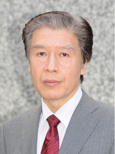
Shigehisa Arai
Shigehisa Arai was born in Kanagawa Prefecture, Japan, on 16 August, 1953. He received the B.E., M.E., and D.E. degrees in electronics from Tokyo Institute of Technology, Japan, in 1977, 1979, and 1982, respectively.
During his Ph.D. work, he demonstrated room-temperature continuous-wave operations of 1.11–1.67-µm-long wavelength lasers fabricated by liquid-phase epitaxy as well as their single-mode operations under a rapid direct modulation. He joined the Department of Physical Electronics, as a Research Associate in 1982, and became a Lecturer in 1984, an Associate Professor in 1987, and a Professor in 1994, Tokyo Institute of Technology. His current research interests are high-performance lasers and photonic integrated circuits on silicon platforms.
Dr. Arai received an Excellent Paper Award from the IEICE of Japan in 1988, the Michael Lunn Memorial Award from the Indium Phosphide and Related Materials Conference in 2000, prizes for science and technology including a Commendation for Science and Technology from the Minister of Education, Culture, Sports, Science and Technology in 2008, an Electronics Society Award and an Achievement Award from IEICE in 2008 and 2011, respectively. He is a fellow of IEICE, JSAP, and IEEE.
-
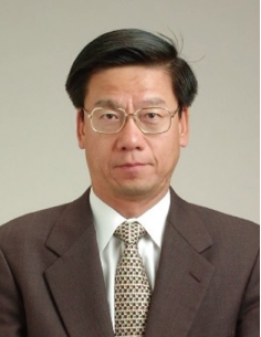
Yoshio Itaya
1981, Received the Ph.D degree in electronics from Tokyo Institute of Technology
1981, Joined the Nippon Telegraph and Telephone Public Corporation (Nippon Telegraph and Telephone Corporation, NTT, at present), engaged consistently in the study of optical semiconductor devices
Jul., 1983 - Jan., 1984, Visiting researcher at the Heinrich Hertz Institute, HHI, West Germany (at the time)
2001, Executive Manager of the Planning Department, NTT Science and Core Technology Laboratory Group
2003, International fellow at the Stanford Research Institute, USA
2004, Vice President, Head of the NTT Photonics Laboratories
2007, Senior Vice President, Head of the NTT Science and Core Technology Laboratory Group
2007, IEEE Fellow
2009, JSAP Fellow
2009-2011, Executive Managing Director of the Photonics Business Group, NTT Electronics Corporation -
Yasuharu Suematsu
Mar.1960, Doctor of Engineering (DE). Electrical Engineering, Tokyo Institute of Technology
Sept.1961-Oct.1973, Associate Professor –Dept. of Electrical Engineering, Tokyo Institute of Technology.
Oct.1967-Sept.1968, Over sea researcher of Ministry of Education and Culture, Japan. At the Electro-Science Lab., Ohio State Univ. U. S. A.
Oct.1973-Oct.1990, Professor- Dept. of Physical Electronics, Tokyo Institute of Technology.
Nov.1983, Valdemar Poulsen Gold Medal, the Danish Academy of Technical Science, for contribution to "the realization of dynamic-single-mode lasers."
Oct.1989-Oct.1993, President - Tokyo Institute of Technology.
Apr.1992-Apr.1993, President –Institute of Electronics, Information and Communication Engineer.
Dec. 1994 Foreign Associate; National Academy of Engineering, USA.
Apr.1995-Mar.1997, Director-General, National Institute for Advanced Interdisciplinary Research, MITI.
Apr.1997-Mar.2001, President, Kochi University of Technology.
May.1997-Apr.2001, Member, Science Council of Japan.
Oct.1997, Eduard Rhein Basic Research Prize, Edward Rhein Foundation, Germany, “for his pioneering work on semiconductor lasers and integrated optics for application in optical communication systems.”
May 2001-May 2002, President, The Institute of Image Information and Television Engineers
Apr.2001-Mar.2005, Director General- National Institute of Informatics.
March 2000, Foreign Member, National Academy of Engineering, Korea.
Apr.2003-Jan.2005, Chairperson, Science and Technology Council, Ministry of Education, Science and Culture.
June 2003, IEEE Medal, James H. Mulligan, Jr. Education Medal, for outstanding leadership in graduate and undergraduate education as mentor, professor and president, and for pioneering contribution to research and education in optical communication devices.
Mar. 2007 Meritorious Member, Institute of Applied Physics of Japan
July.2011-Present, Honorary Professor, Tokyo Institute of Technology
April 2014, Japan Prize, the Japan Prize Foundation, for his “pioneering research on semiconductor lasers for high-capacity, long-distance optical fiber communication”.
Nov. 2015, The Order of Culture, from Emperor of Japan -
Katsumi Kishino
Katsumi Kishino earned his Bachelor’s, Master’s, and Doctorate degrees in Engineering from the Tokyo Institute of Technology, Tokyo, Japan, in 1975, 1977, and 1980, respectively. From 1980 to 1984, he was a Research Associate at Tokyo Institute of Technology. In 1984, he joined the Department of Electrical and Electronics Engineering, Sophia University, Tokyo, as a Lecturer. Then, he was appointed as an Associate Professor in 1986 and a Professor in 1992. He has engaged on the research of GaInP-based red laser diodes, novel II-VI compounds on InP substrates and related yellow-green emitters. Currently, he is conducting research on nitride semiconductors by rf-MBE including GaN-based nanocolumn, InGaN-based full-color nanoemitters, and InN-related materials. From Sept. 1989 to Aug. 1990, he worked on the first stage of research of resonant-cavity-enhanced (RCE) photodetectors as a Visiting Associate Professor at the University of Illinois at Urbana-Champaign, on leave from Sophia University. Dr. Kishino is a fellow of JSAP, IEICE, and IEEE.
K.Kishino, M.Itaya, S.Arai, T.Kanayama(Organizing Committee Chair)
History of the SSDM Award is here
SSDM Paper Award
SSDM Paper Award2016 will be awarded to the best paper presented at SSDM2015.
-
Presentation No. K-2-4 [Area 3]Steep-Slope Tunnel FET using InGaAs-InP Core-Shell Nanowire/Si HeterojunctionK. Tomioka1,2, F. Ishizaka1, J. Motohisa1, T. Fukui1
(1Hokkaido Univ., 2JST-PRESTO (Japan))

T.Fukui, J.Motohisa, F.Ishizaka, K.Tomioka, T.Kanayama(Organizing Committee Chair)
SSDM Young Researcher Award
SSDM Young Researcher Award 2016 will be awarded to outstanding papers authored by young researchers and presented at SSDM2015.
-
Presentation No.N-2-2 [Area 1]Ω-Gate Nanowire Transistors Realized by Sidewall Image Transfer Patterning: 35nm Channel Pitch and Opportunities for Stacked-Nanowires ArchitecturesL. Gaben1,2,3, S. Barraud1, P. Pimenta-Barros1, Y. Morand2, J. Pradelles1, M.P. Samson2, B. Previtali1, P. Besson2, F. Alain1, S. Monfray2, F. Boeuf2, T. Skotnicki2, F. Balestra3, M. Vinet1
(1CEA-LETI, 2STMicroelectronics, 3IMEP-LAHC) -
Presentation No.O-4-4 [Area 5]Area-Efficient Non-volatile Carry Chain Based on Pass-Transistor/Atom-Switch Hybrid LogicX. Bai, Y. Tsuji, A. Morioka, M. Miyamura, T. Sakamoto, M. Tada, N. Banno, K. Okamoto, N. Iguchi, H. Hada
(NEC Corp.) -
Presentation No.G-5-3 [Area 8]Thermally-Stable High Sn Concentration (~9%) GeSn on Insulator by Ultra-Low Temperature (~180°C) Solid-Phase Crystallization Triggered by Laser-Anneal SeedingR. Matsumura1,2, K. Moto1, Y. Kai1, T. Sadoh1, H. Ikenoue1, M. Miyao1
(1Kyushu Univ., 2JSPS Research Fellow) -
Presentation No.F-7-3 [Area 11]In situ Monitoring of Extracellular Matrix Based on Chondrocytes Behavior using Biologically-coupled Field Effect TransistorH. Satake1, A. Saito1, T. Kajisa2, S. Mizuno3, T. Sakata1
(1Univ. of Tokyo, 2PROVIGATE Inc., 3Harvard Medical School) -
Presentation No.P-3-5 [Area 12]Millimeter-Wave Detector Using Magnetic Tunnel Junctions With Perpendicularly Magnetized L10-Ordered FePd Free LayerK. Mukaiyama1, H. Naganuma1, T. Yu1, H. Kubota2, A. Fukushima2, M. Oogane1, Y. Ando1
(1Tohoku Univ., 2AIST) -
Presentation No.D-3-6L [Area 13]Direct Evidence of Defect-defect Correlation in Atomically Thin MoS2 Layer by Random Telegraphic Signals Observed in Back-gated FETsN. Fang, K. Nagashio, A. Toriumi
(Univ. of Tokyo)
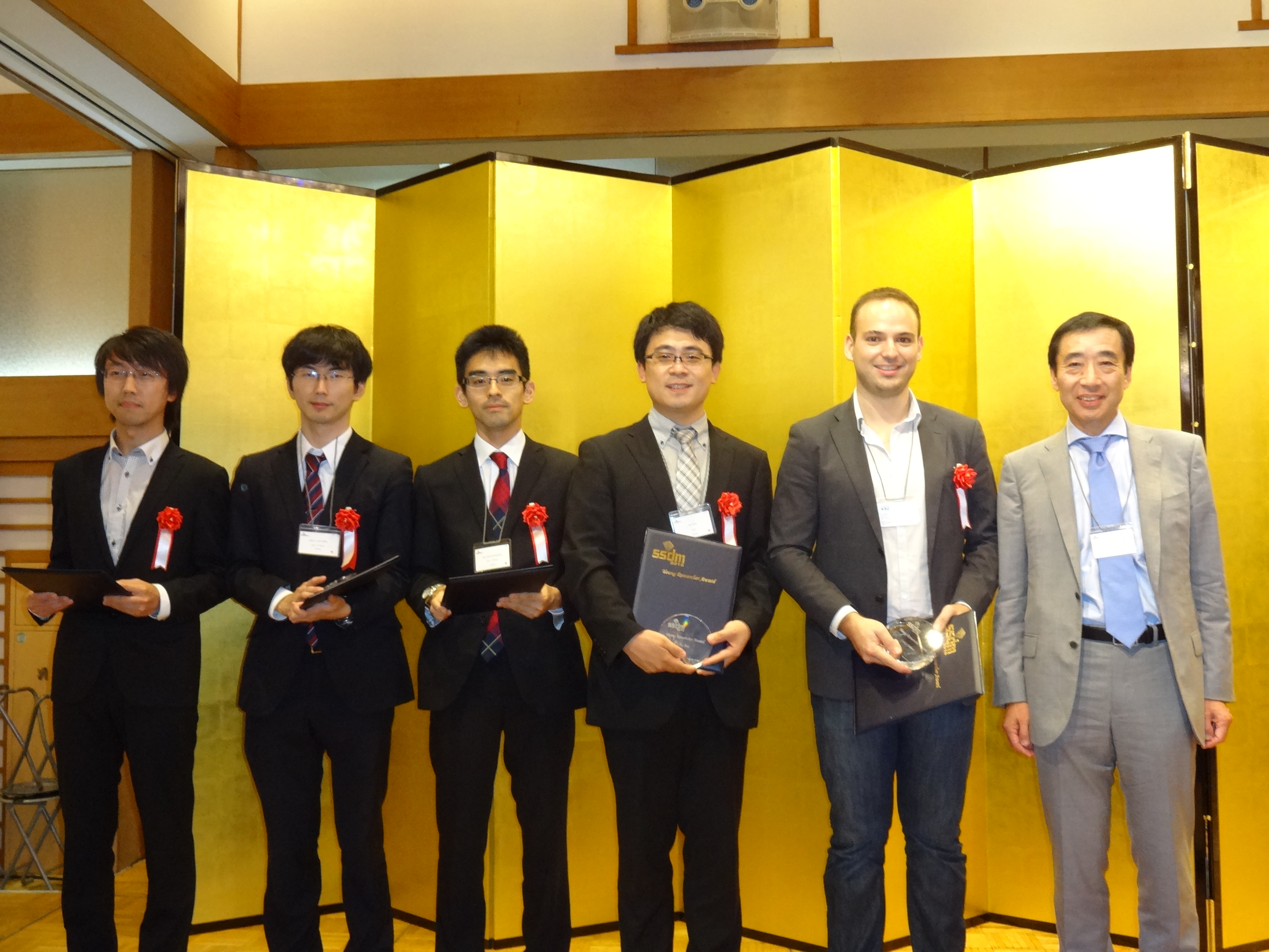
N.Fang, H.Satake, R.Matsumura, X.Bai, L.Gaben, T.Kanayama(Organizing Committee Chair)
Call for 2016 SSDM Award Nomination
The SSDM Award was established to recognize outstanding contributions to academic or industrial development in the field of solid state devices and materials.
Papers to be nominated for the 2016 SSDM Award should be among those that have been presented between the 1st SSD conference in 1969 and the 42nd SSDM conference in 2010.
The SSDM Award will ultimately be decided by the SSDM Organizing Committee after a recommendation is made by the SSDM Award Nomination Committee.
The recommendation will be in accordance with the following two criteria.
-
1) Originality
The award-winning selection must be original, and must have had significant theoretical or practical impact in the field of solid state devices and materials.
-
2) Contribution
The author(s) of the award-winning selection must have played or be playing a pioneering or leading role, with globally outstanding contributions in the technological field.
Candidate and Nominator Eligibility
-
- Candidates Eligible for the Award
All authors who presented papers between the 1st SSD conference in 1969 and the 42nd SSDM conference in 2010, excluding papers written by this year’s Organizing Committee Chair.
-
- Persons Eligible for Nominating Candidates
Anyone, excluding this year's members of the SSDM Award Nomination Committee
Submission Process for SSDM Award nominations
The following is the process for submitting nominations.
- - Before deciding on a candidate for the award, confirm the eligibility of nominators and candidates once again.
- - Download the Nomination Form
SSDM Award Nomination Form [MS-Word]. - - Fill out the Nomination Form and send it to the SSDM Secretariat by the nomination deadline.
Nomination deadline: March 31, 2016 Closed
If you have any questions, please ask the secretariat by e-mail
Sumitomo-Shoji Kanda-Izumi-cho Bldg., 13F
1-13 Kanda-Izumi-cho, Chiyoda-ku, Tokyo 101-0024
closed on March 31.