Award
SSDM Award
The SSDM Award is awarded to researchers who contributed an outstanding paper at past SSDM. The Award Committee selects this award.
This paper was the first report of a practical vertical MOSFET with high breakdown voltage and high current drivability. Since then, many vertical structure devices such as trench-gate MOSFETs, super-junction (SJ) MOSFETs, and insulated gate bipolar transistors (IGBTs) based on this structure have been developed. Therefore, it can be said that this paper was one of the key factors for the realization of today’s power devices.
In the 1970s, when this paper was published, silicon MOSFETs had low current drivability and their process technology was immature, so silicon bipolar devices were widely used as power devices. On the other hand, at the research level, the idea of a “V-MOS” with a vertical structure that flowed current through a chip along a V-shaped groove had been proposed and intensively studied in an attempt to improve the current drivability. However, the V-MOS had reliability problems due to the electric field concentration at the gate tip in addition to a difficult fabrication process, so it has never been used in commercial products.
In this paper, the authors proposed combining the planar gate structure and the vertical structure to provide high current drivability, and they employed a mesh-gate structure to reduce the parasitic resistance and capacitance. They fabricated prototype devices and demonstrated their excellent characteristics.
Today, with the growing interest in environmental issues, power devices are becoming more important as a key to reducing energy consumption. The vertical MOS structure derived from this paper is not only used in the majority of silicon power MOSs and IGBTs, but is also essential for the next generation of power devices using new materials such as SiC and GaN, which are currently being intensively studied.
From the above, this paper is recognized as having made a significant contribution to the academic achievement of transformation of power device structures and their development as an industrial technology. Therefore, the SSDM Award is presented to the authors of this paper in recognition of their achievements.
-

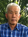
Isao Yoshida
NPO Analog Technology NetworkIsao Yoshida graduated from Shizuoka Technical High School in 1965, and graduated from Hitachi Technical College in 1968. He was at the University of Tokyo as a visiting researcher from 1968 to1969. He received the Ph.D. degree from Tokyo Institute of Technology, Tokyo, Japan, in 1984. He joined the Central Research Laboratory of Hitachi, Ltd. in 1965. He had been engaged in developing power MOSFETs and RF modules for 30 years. He moved to the Renesas Tchnology, Ltd. from the Hitachi, Ltd. in 2002. He retired the affiliation and joined the NPO Analog Technology Network in 2004. Dr. Yoshida received the Ohm Technical Award in 1991. He received the SSDM Award (Title of paper; Properties of MOS Structured on Substrates Having Ion-implanted Impurity Distribution Profile) in 2000. He received the Ichimura Industrial Award in 2003.
-

Masaharu Kubo
Former Hitachi Ltd.-
(Academic Carriers)
- March, 1962 BSEE, Hokkaido University
- June, 1971 MSEE, Stanford University
- June, 1973 Dr. of Engineering, Hokkaido University
-
(Occupation Carriers)
- 1. Present from June 2003 Individual business named as MK Innovation and 1H 3H Co. Renewable Energy
- 2. 2003 from 1985 Deputy General Manager and Chief Engineer at Semiconductor Group of Hitachi Co.
- 3. 1985 form 1962 Department Manager, Senior Researcher and Researcher at Central Research Lab. of Hitachi Co.
-
(Technical Carriers)
- 1. Power MOS FETs for Switching Regulators
- 2. CCD and MOS Imaging Devices for Video Camera
- 3. MOS FETs and MOS LSI for Consumers (Smart Phone) and for Industries (Personal Computers), Specifically for Protection Schemes of their Gate Electrodes against Static Damages
-
(Awards outsides from Hitachi Corporation (The only significant ones are remarked.))
- (1) IEEE Life Fellow (2007).
- (2) IEEE Millennium Award (2000).
- (3) Director Award of Science and Technology Ministry in Japan (1999).
- (4) Edward Rhein Award (1980)
Note: This award is often called as Nobel prize in Consumer Electronics.
This prize were bestowed to 4 Japanese Engineers (Hitachi and Sony) contributing to the development of solid state image sensors for digital cameras. - (5) Ichimura Prize (1973,1989)
-
(Academic Carriers)
-
Shikayuki Ochi
SSDM Young Researcher Award
SSDM Young Researcher Award is awarded to outstanding papers authored by young researchers and presented at SSDM in the previous year.
Univ. of Tokyo (Japan)
D. Löhr, R. Hoffmann, M. Czernohorsky, K. Kühnel, P. Steinke, K. Zimmermann,
K. Biedermann, K. Seidel, J. Müller
Fraunhofer IPMS Center Nanoelectronic Technologies (Germany)
1.Univ. of Tsukuba (Japan), 2.MIT (USA), 3.Saga Univ. (Japan)
M. Hayama, H. Oka
Panasonic Corp. (Japan)
K. Matsuda2, Y. Miyauchi2, T. Takenobu1
1.Nagoya Univ. (Japan), 2.Kyoto Univ. (Japan), 3.Tokyo Metropolitan Univ. (Japan), 4.KAUST (Saudi Arabia)
Univ. of Tokyo (Japan)
S. Steudel1, J. Genoe1,2, P. Heremans1,2, K. Myny1
1.imec (Belgium), 2.KU Leuven (Belgium)
Tohoku Univ. (Japan)
Call for 2019 SSDM Award Nomination
The SSDM Award was established to recognize outstanding contributions to academic or industrial development in the field of solid state devices and materials.
Papers to be nominated for the 2019 SSDM Award should be among those that have been presented between the 1st SSD conference in 1969 and the 45th SSDM conference in 2013.
The SSDM Award will ultimately be decided by the SSDM Organizing Committee after a recommendation is made by the SSDM Award Nomination Committee.
The recommendation will be in accordance with the following two criteria.
-
1) Originality
The award-winning selection must be original, and must have had significant theoretical or practical impact in the field of solid state devices and materials.
-
2) Contribution
The author(s) of the award-winning selection must have played or be playing a pioneering or leading role, with globally outstanding contributions in the technological field.
Candidate and Nominator Eligibility
-
- Candidates Eligible for the Award
All authors who presented papers between the 1st SSD conference in 1969 and the 45th SSDM conference in 2013, excluding papers written by this year’s Organizing Committee Chair and Award Nomination Committee Chair.
-
- Persons Eligible for Nominating Candidates
Anyone, excluding this year’s members of the SSDM Award Nomination Committee
Submission Process for SSDM Award Nominations
The following is the process for submitting nominations.
- - Before deciding on a candidate for the award, confirm the eligibility of nominators and candidates once again.
- - Download the Nomination Form.
SSDM Award Nomination Form (MS-Word) - - Fill out the Nomination Form and send it to the SSDM Secretariat by the nomination deadline.
The deadline for nomination is now extended till May 27, 2019. CLOSED
If you have any questions, please ask the secretariat by e-mail
Sumitomo-Shoji Kanda-Izumi-cho Bldg., 12F
1-13 Kanda-Izumi-cho, Chiyoda-ku, Tokyo 101-0024


