Awards
SSDM Award
2 CREST, Japan Science & Technology Corporarion (JST)
3 Department of Precision Science and Technology, Osaka University
This study verified the use of solid-state electrochemical reaction in electrically establishing a quantum point contact switch. This laid an innovative foundation for non-volatile solid-state atomic switch, a technology that has started to be applied commercially in areas such as FPGA (Field-Programmable Gate Array).
Until the release of this paper, quantum point contact switches had been explored based on electrical characteristics of ultra-small semiconductor devices operating at ultra-low temperatures or by way of mechanically controlling the vertical movements of STM (Scanning Tunneling Microscope), but these could not deliver practical application as integrated circuit elements. The authors brought silver nanowires, coated with silver sulfide, close to a platinum electrode to confirm that (1) applying a negative bias to platinum-precipitated silver atoms, forming an atomic bridge between both electrodes, that (2) applying a reverse bias erased the atomic bridge and that (3) quantization of electrical conductance pointed to the formation of a quantum point contact. Some of these findings have been released to “Riken Review.” In the SSDM2001, with regard to atomic-level structural changes from electrical control, which is a key factor in the composition of atomic switch, the authors (1) used SEM (Scanning Electron Microscope) to confirm that applying bias to a nano-bridge, formed with electrochemical reaction, produced protrusion of silver nano particles at the tip, and (2) confirmed that STM could be used to regulate the protrusion of silver nano-particles at the tip according to the bias. These findings show that the hurdles against practical application of atomic switch have finally been cleared.
The authors have subsequently engaged in joint research with private enterprise to examine material / device structures, and precipitate / erase copper nano-bridge within copper sulfide to achieve “switching elements as fully solid-state elements” with significantly-improved reliability. This represents a major contribution to the highly-anticipated development of electronic devices for practical use, such as FPGA for highly functional AI (Artificial Intelligence) and electron devices for space applications with strong radiation resistance.
As described, this paper provided technical contents that could convert academic discovery into industrial use as electron devices for integrated circuits. It is therefore recognized as being deserving of the SSDM Award. We hereby present the SSDM Award in recognition of their achievement.
-
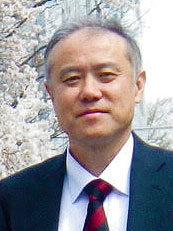
Tsuyoshi Hasegawa
Waseda UniversityTsuyoshi Hasegawa is a professor of Department of Applied Physics, Waseda University. He received the B.S. degree in Physics in 1985, the M.S. degree in Materials Science in 1987, and the Ph.D. degree in Physics in 1996 from the Tokyo Institute of Technology. He worked for Hitachi Ltd. at the Central Research Laboratory from 1987 to 1999. He joined the RIKEN (the Institute of Physical and Chemical Research) in 1999 as a senior researcher, and the NIMS (National Institute for Materials Science) in 2002 where he led the Atomic Electronics Group as a group leader. He became a Principal Investigator of the International Center for Materials Nanoarchitectonics (MANA) in 2007. After that, he became a professor of Waseda University in 2015. He has conducted several national research projects, such as JST/CREST (2009-2015).
-
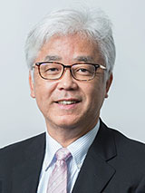
Kazuya Terabe
National Institute for Materials Science (NIMS)Kazuya Terabe received the B.S. degree in 1986, the M. S. degree in 1988, and Ph.D degree in 1992 in materials science and engineering from Nagoya Institute for Technology. He was a research associate at Nagoya University in 1992, was a special postdoctoral researcher at RIKEN in 1996 and started the nanoionics research. He joined National Institute for Materials Science (NIMS) in 2001 and is currently a Principal Investigator & Group Leader at the MANA International Center. His research interests are the creation and practical application of nanoionics devices such as neuromorphic devices and atomic switches that operate by local ion transfer in solids.
Dr. Terabe is a vice-chair of area 9-SSDM in 2020 and became a fellow of the Japan Society of Applied Physics in 2020. He received the commendation for Science and Technology by the Minister of Education, Culture, Sports, Science and Technology in 2007, and Tsukuba Prize in 2017. -
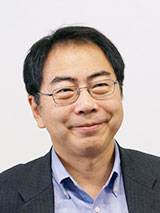
Tomonobu Nakayama
National Institute for Materials Science (NIMS)Tomonobu Nakayama is the Deputy and Administrative Director and also a Principal Investigator at International Center for Materials Nanoarchitectonics (WPI-MANA), National Institute for Materials Sceince (NIMS), and also a Professor at University of Tsukuba. He graduated and received his master’s degree from Tokyo Institute of Technology (1988), and later received a PhD in physics from the University of Tokyo (1999). He worked for Mitsui Mining & Smelting Co. Ltd., JRDC (former JST), RIKEN, and moved to NIMS in 2002. In recent years, He has been investigating functionalities of integrated nanomaterial systems such as ultrahigh density data storage with single-molecule-level memories, and neuromorphic materials integration for brain-like information processing. He believes that a development of new methodology and technology at the nanometer regime is essential to open a new paradigm of nanoscience and nanotechnology, i.e., he developed a multiple-probe scanning probe microscope.
-
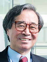
Masakazu Aono
National Institute for Materials Science (NIMS)Masakazu Aono is Executive Advisor (former Director) of International Center for Materials Nanoarchitectonics (MANA), National Institute for Materials Science (NIMS), Japan. He received his PhD from University of Tokyo in 1972 and then worked at National Institute for Research in Inorganic Materials (NIRIM) as Research Scientist (1972–86), Institute for Physical and Chemical Research (RIKEN) as Chief Scientist (1986–2002) and Osaka University as Professor (1996–2005). During that period, he was concurrently Visiting Professor of University of Wisconsin (USA) (1978–80), Visiting Scientist of IBM Watson Research Center (USA) (1978–80).
He is a pioneer of nanoscale science and technology; he was described as “Leader in Atomic-scale Control and Nano-manipulation” in a journal of American Chemical Society (ACS Nano 1 (2007) 397); when he received Feynman Prize of Nanotechnology (USA) in 2010, the reason for his receiving the prize was: “ - - in recognition of his pioneering and continuing work, - - and his inspiration of an entire generation of researchers who have made their own ground-breaking contributions to nanotechnology”.
SSDM Paper Award
2 Univ. of Yamanashi
-
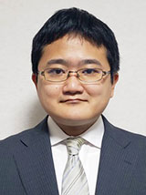
Ryo Tanaka
Fuji Electric Co., Ltd.Ryo Tanaka was born in Nagoya, Japan, in 1984. He received the B.S. degree in Physical Science and Engineering, and the M.S. degree in Crystalline Materials Science, both from Nagoya University, Aichi, Japan, in 2007 and 2009, respectively. When he was a graduate school student at Nagoya University, he studied a bulk crystal growth of SiC using solution method.
Since 2009, he has been with Fuji Electric Co., Ltd., Tokyo, Japan, where he has engaged in research on microcrystalline Si solar cell, GaN HEMTs, and GaN MOSFETs. From 2014 to 2016, he was a Visiting Research Scholar with University of California, Santa Barbara, where he studied the device processing and epitaxial growth of GaN. He is currently working on the development of vertical GaN MOSFETs. He is a member of JSAP. -
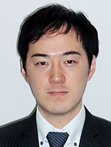
Shinya Takashima
Fuji Electric Co., Ltd.Shinya Takashima received the B.S. degree in applied chemistry and the M.S. and Ph.D. degrees in materials science from Tokyo University, Tokyo, Japan, in 2002, 2004, and 2007, respectively.
Since 2007, he has been with Fuji Electric Co. Ltd., Tokyo, Japan. Since 2009, he has been working on research and development of GaN power devices. From 2011 to 2013, he was a Visiting Research Scholar in Rensselaer Polytechnic Institute, Troy, NY, where he studied the device processing and characterization of lateral GaN power devices, and optimization of the GaN MOS interface. His current research focuses on the vertical GaN power MOSFETs and relating process developments. He is a member of JSAP and IEEE. -
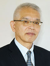
Katsunori Ueno
Fuji Electric Co., Ltd.Katsunori Ueno was born in Fukuoka, Japan, in 1957. He has joined Fuji Electric Co. Ltd., Tokyo, Japan since 1982, and has been engaged in the development of IGBTs for power applications, and has also developed FS-IGBTs, RB-IGBTs and the super-junction MOSFETs. From 1990, he has started SiC device-application technologies especially on the ion-implantation and on the MOS interfaces. He received Ph.D. degree in engineering from Yamanashi University, Yamanashi, Japan, in 1996. From 2009, he joined the project for power GaN-HEMTs between Furukawa Electric and Fuji Electric. His current work is development of GaN vertical devices. He is a member of JSAP.
-
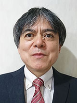
Hideaki Matsuyama
Fuji Electric Co., Ltd.Hideaki Matsuyama was born in Hokkaido, Japan, in 1955. He graduated from the Department of Physics at Hokkaido University, Hokkaido, Japan in 1979 and completed his Master's degree in Applied Physics at Hokkaido University in 1981. From 1981 to 1990, he worked for Sony Corporation, Tokyo, Japan. Since 1990, he has been with Fuji Electric Co., Ltd., Tokyo, Japan, where he has involved in the development of solar cells, hard disk media, etc. He is currently working on the development of GaN MOSFETs.
-
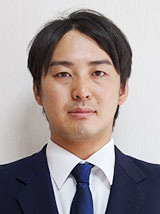
Yuta Fukushima
Fuji Electric Co., Ltd.Yuta Fukushima was born in Kagoshima, Japan, in 1991. He received the B.S. in 2014 and the M.S. in 2016 in Materials Science and Engineering from Kyushu University, Fukuoka, Japan. In Master’s project, he committed himself in grain refinement and phase transformation of materials by high-pressure deformation processing. From 2014 to 2015, he was an exchange scholar at Arizona State University, USA, where he focused on atomic-resolution TEM analysis for direct observation of metastable phases.
He joined Fuji Electric Co., Ltd., Tokyo, Japan in 2016 and has engaged in development of GaN MOSFETs from 2017 to 2020. Currently, he is working on TEM analysis of IGBTs, MOSFETs, and magnetic recording devices. He is a member of JSAP. -
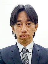
Masaharu Edo
Fuji Electric Co., Ltd.Masaharu Edo was born in Tokyo, Japan, in 1969. He received the B.S. degree in Faculty of Science and Technology from Tokyo University of Science, Chiba, Japan, in 1993. When he was a graduate school student at Tokyo University of Science, he studied a Si semiconductor design and process.
Since 1993, he has been with Fuji Electric Co., Ltd., Tokyo, Japan, where he has engaged in research on Micro Electro Mechanical Systems, Magnetic Devices, Mgnetic Materials. From 2009, he joined the project for power GaN-HEMTs between Furukawa Electric and Fuji Electric. He is currently working on the development of vertical GaN MOSFETs. -
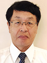
Kiyokazu Nakagawa
Tokyo City University / Abit Technologies Co., Ltd.WORK EXPERIENCE
April 1981 – March 2000; Researcher of Central Research Laboratory, Hitachi Ltd.
April 2000 – March 2017; Professor of Yamanashi University
April 2017; Emeritus Professor of Yamanashi University
April 2017 – March 2019; Researcher of donation course from Fuji Electric Co., Ltd. at Yamanashi University
April 2019 – present; Visiting Professor of Tokyo City University, CTO of Abit Technologies Co., Ltd.
To defeat problems with the miniaturization in the Si ULSIs, Si-related heterostructure formation technologies were developed. Impurity delta doping was realized and transistors with delta doped structures were demonstrated. Single crystal CoSi2 layers were successfully grown on Si substrates and the transistors with the buried gate electrodes of CoSi2 showed ultra-high-speed operation. The high electron and hole mobility devices with SiGe heterostructures were realized.
In addition, the forming technology of high-quality gate insulator of SiO2 for GaN was developed.
EDUCATION
April 1978 – May 1981; University of Tokyo, doctoral course
May 1981; PhD in Engineering
SSDM Young Researcher Award
-
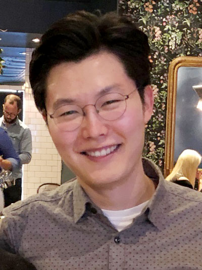
Junkyo Suh
Stanford UniversityJunkyo Suh received the B.S. degree from Yonsei University, Seoul, South Korea in 2009, and M.S. degree from the University of Tokyo, Tokyo, Japan in 2011. He is currently pursuing the Ph.D. degree in electrical engineering at Stanford University, CA. His Ph.D. dissertation primarily focuses on SiGe and/or Ge nanowire platform for nanoelectronics and nanophotonics. His current research interests include novel materials and device architectures for optoelectronics. From 2012 to 2015, he was a research engineer for South Korea’s mandatory military service at SK Hynix, Icheon, South Korea, where among many he was involved in technologies for DRAM and new types of storage class memory (SCM).
-
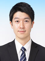
Jun Tsunoda
Waseda UniversityJun Tsunoda was born in Yamanashi, Japan, in 1996. He received the B.Eng. degree in electronic and physical systems from Waseda University, Tokyo, Japan. Currently, he is a M.Eng. student in the department of electronic and physical systems at Waseda University. His research interests include singlecrystalline diamonds, crystal growth, etching, metal-oxide-semiconductor field-effect transistors, power devices and complementary MOS inverters. He received the Best Poster Session Award in the 32nd Diamond Symposium in 2018, Tokyo, Japan.
-
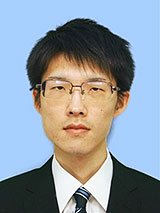
Shota Urayama
Tohoku UniversityApril 2012 – March 2015, Toyama Chubu High School, Toyama, Japan April 2015 – March 2019, Department of Mechanical and Aerospace Engineering, School of Engineering, Tohoku University, Sendai, Japan April 2019 – present, Graduate School of Biomedical Engineering, Tohoku University, Sendai, Japan
-
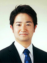
Naoki Higashitarumizu
The University of TokyoNaoki Higashitarumizu received the B.S., M.S., and Ph.D. degrees in materials engineering from The University of Tokyo in 2015, 2017, and 2020, respectively. He was a postdoctoral fellow at The University of Tokyo from April to September 2020. Currently, he is a postdoctoral fellow at the University of California at Berkeley. His research focuses on the optical and electronic properties of novel layered semiconductors.
-

Tomotaka Hirano
Hiroshima UniversityTomotaka Hirano was born in Tokushima, Japan, in 1995. He received the B.E. and M.E degrees of semiconductor electronics from Hiroshima University under the guidance of Professor Seiichiro Higashi, in 2018 and 2020, respectively. He had been engaged in research on flexible hybrid electronics and demonstrated fabrication of high-performance single-crystalline Silicon devices on PET substrate at a low process temperature with the yield of over 99.9%. After completing the M.E. program, he joined Tokyo Electron Miyagi Limited in 2020 and has been engaged in research and development of dry etching process for advanced devices.
-
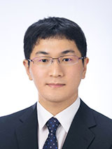
Kohei Matsuda
Kobe University (– 2020.03)
Sony Semiconductor Solutions Corporation (2020.04 –)Kohei Matsuda received the B.E., M.E. and Ph.D. degrees in computer science from Kobe University, Kobe, Japan, in 2015, 2017, and 2020, respectively. During his degrees, he was involved in a research project developing circuit-level countermeasure against physical attacks and design methodology for cryptographic processors.
In 2020, he joined Sony Semiconductor Solutions Corporation, Atsugi, Japan, where he has been involved in the research and development of advanced CMOS image sensors.
Call for 2020 SSDM Award Nomination
The SSDM Award was established to recognize outstanding contributions to academic or industrial development in the field of solid state devices and materials.
Papers to be nominated for the 2020 SSDM Award should be among those that have been presented between the 1st SSD conference in 1969 and the 46th SSDM conference in 2014.
The SSDM Award will ultimately be decided by the SSDM Organizing Committee after a recommendation is made by the SSDM Award Nomination Committee.
The recommendation will be in accordance with the following two criteria.
-
1) Originality
The award-winning selection must be original, and must have had significant theoretical or practical impact in the field of solid state devices and materials.
-
2) Contribution
The author(s) of the award-winning selection must have played or be playing a pioneering or leading role, with globally outstanding contributions in the technological field.
Candidate and Nominator Eligibility
-
- Candidates Eligible for the Award
All authors who presented papers between the 1st SSD conference in 1969 and the 46th SSDM conference in 2014, excluding papers written by this year’s Organizing Committee Chair and Award Nomination Committee Chair.
-
- Persons Eligible for Nominating Candidates
Anyone, excluding this year’s members of the SSDM Award Nomination Committee
Submission Process for SSDM Award Nominations
The following is the process for submitting nominations.
- - Before deciding on a candidate for the award, confirm the eligibility of nominators and candidates once again.
- - Download the Nomination Form.
SSDM Award Nomination Form (MS-Word) - - Fill out the Nomination Form and send it to the SSDM Secretariat by the nomination deadline.
The deadline for nomination has been extended till April 24, 2020. CLOSED
If you have any questions, please ask the secretariat by e-mail
Sumitomo-shoji Kanda-Izumi-cho Bldg.,12F,
1-13 Kanda-Izumi-cho Chiyoda-ku Tokyo, Japan 101-0024


