

Awards
SSDM Award
2) Hitachi Microcomputer Engineering, Ltd.,
3) Kanagawa Works, Hitachi, Ltd.
This is an advanced study on the degradation or dielectric breakdown of gate insulating film caused by dry etching, which is a main processing technology used for producing LSI chips. This is, in fact, the first paper in the world to report the so-called “antenna effect,” concerning MOS dielectric breakdown with a focus on the ratio between MOS area and the size of the connected pad. It has set a basic guideline on how to develop damage-less dry etching devices, significantly accelerating the subsequent development of ultra-small semiconductor devices.
Compared with other processing technologies, dry etching has excellent micro/nano-fabrication performance and material selectivity. For this reason, to this day, it remains to be one of the key technologies that help semiconductor devices become miniaturized with greater integration. In the early 1980s, when there was a shift from wet to dry etching due to microfabrication limits involved in the wet process, the industry began to face the degradation and breakdown of insulating films caused by charging damage during plasma etching (plasma damage), which had never been an issue before. It was initially suspected that the insulating films suffered characteristic degradation and dielectric breakdown because of localized high electric field caused by switching during plasma generation for use in dry etching, followed by charge buildup in the film. This paper made systematic and experimental considerations concerning charge storage and thickness dependency of gate insulating film in degradation or breakdown, using a barrel-type plasma etcher, and concluded that dielectric breakdown was caused by current stress during etching, rather than a high electric field momentarily applied to the film. Beyond that, this is also recognized as the world’s first report about the “antenna effect” concerning MOS dielectric breakdown by plasma damage with a focus on the ratio between MOS area and the size of the connected pad. Then this paper had inspired active further research into plasma damage not only by this paper’s research team, but also by a number of industries and universities, resulting in the improvement and enhancement of plasma etchers. The “antenna effect” also strongly suggested that circuit patterns could affect the dielectric breakdown of MOS, which had led to the industry’s move to a constraint in design rule checking on dangerous layout patterns that could cause the antenna effect, thus averting defective products in mass production.
As explained above, this paper has made an extremely significant contribution to the deployment of microfabrication technology through the R&D of dry-etching technology, which supports today’s semiconductor industry. It also has a highly advanced level of academic value from the perspective of establishing reliability physics of MOS dielectric breakdown. In recognition of these achievements, we hereby present the SSDM Award to this paper.
-
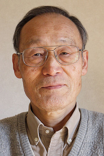
Kazuyuki Tsunokuni
MICRONICS JAPAN CO., LTD.Kazuyuki Tsunokuni received the B.S. degree in physics from Tokyo University of Science in 1979 and the M.S. degree in physics from Tohoku University in 1982.
He joined Hitachi, Ltd. in 1982 and was engaged in the development of a new isolation process for DRAM in Musashi Works.
He started a study on the charge build-up during plasma process in 1984 and found an evaluation method and a model of gate oxide breakdown during plasma process.
After that, he had been evaluating the charging damage of almost all the dry etchers and several ion implanters.
From 1996 to 1998, he worked on the dry etching process for Twinstar Semiconductor Inc. in Texas.
After returning to Japan, he was engaged in the yield enhancement for SOCs and Zero Defect project for automotive MCUs in Naka Factory.
He retired from Renesas Electronics Corp. in 2012, and joined MICRONICS JAPAN CO., Ltd. in 2013
He worked on the R&D of the solid-state secondary battery until 2020 and currently belongs to Corporate Planning & Strategy Division. -
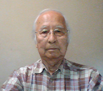
Kazuo Nojiri
Nanotech ResearchKazuo Nojiri is a President of Nanotech Research. He has 46 years of experience in semiconductor industry. He joined Hitachi Ltd. in 1975, where he held numerous management positions in Dry Etching and Device Integration. At Hitachi, he began his career working on Plasma CVD, then engaged in the development of Plasma Etching. He is also known as a pioneer in the research field of charging damage. He joined Lam Research Co., Ltd. in 2000, where he was a CTO until 2016 and became a Fellow in 2017. After leaving Lam in 2018, he has been working as a consultant, and provides Business and Technology solutions. He published 39 technical papers. He has published the book entitled “Dry Etching Technology for Semiconductors” (Springer, 2015). He holds 58 patents, including 33 US patents. In 1989, he was awarded the Okouchi Memorial Prize for the development of ECR plasma etching technology. In 2019, he received the DPS Nishizawa Award. He has served as a member of organizing committee and program committee in various conferences.
-
Sumi Kuboshima
Sumi Kuboshima received the B.S. degree in physics from Yamanashi University in 1985.
She joined Hitachi-Microcomputer Engineering, Ltd. in 1985 where she worked on study of charging polarity during dry etching for submicron device.
She also evaluated dry etching charge-up depend on the area ratio of gate layer and metal one and the implant damage for transistor characteristics for 3 years.
After that, she left the company in 1988. -
Kado Hirobe
In 1970, join in Hitachi Co. , Semiconducter Dev. (Tokyo), working for development of semiconductor technology.
In 1989, join in ROHM Co (Kyoto)
In 1992, join in Matsusita Works Co.(Panasonic Co.) (Osaka)
In 2003, join in Micromachine center(Tokyo), working for National Project of MEMS technology(METI)
After 2007, being involved in voluntary activity concerned in Mega solar power generation on Lake Biwa.
“A sustainable community designed by Lake Biwa – Shiga model” published in 2017, Amazon Kindle edition.
SSDM Paper Award
2 Toshiba Information Systems (Japan) Corporation
-
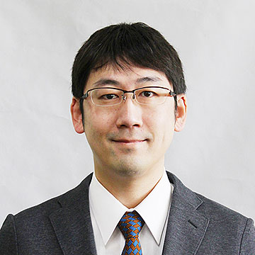
Takao Marukame
Toshiba CorporationTakao Marukame was born in Sapporo, Japan, in 1978. He received the B.E. and M.E degrees in Engineering, and the Dr. (Eng.) degree in Information Science and Technology from Hokkaido University, Hokkaido, Japan in 2002, 2004 and 2007, respectively. Since 2007, he has been with Toshiba Corporation, Kawasaki, Japan, where he has engaged in research on advanced LSI technology, spintronic devices and memory systems. From 2014 to 2015, he was a Visiting Scientist at Ecole Polytechnique Federale Lausanne (EPFL), Lausanne, Switzerland, where he studied microelectronic circuits and systems. He is currently working on the development of neuromorphic and brain-inspired devices. He is a member of JSAP and IEEE.
-
Koichi Mizushima
Toshiba CorporationKoichi Mizushima received the B.S., M.S. and the Ph.D. degrees in solid state physics from Tokyo Univ. in 1964, 1966 and 1969, respectively. From 1964 to 1981 at Tokyo Univ., he did mainly basic researches concerning magnetostriction, hopping-conduction and metal/insulator transitions in transition-metal oxides. In 1978 and 79, he stayed at Inorganic Chemistry Laboratory in Oxford, and developed new cathode-materials for secondary lithium-batteries. From 1982 to 2018 at R & D Center, Toshiba Corporation, Kawasaki, Japan, he has done various researches such as molecular electronics using Langmuir-Blodgett films, high-temperature superconducting devices, spin-valve transistors, and spin-transfer microwave nano-oscillators applied to magnetic recording heads. From 2019, he is developing hardware for neuromorphic neural networks.
-
Kumiko Nomura
Toshiba CorporationKumiko Nomura received the B.E degree in information Science and M.E and the Dr. (Eng.) degrees in Communications and Integrated Systems from Tokyo Institute of Technology, Tokyo, Japan in 2000, 2002, and 2005, respectively. Since 2005, she has been with Toshiba Corporation, Kawasaki, Japan, where she has engaged in research on advanced LSI technology systems. She is currently working on the development of neuromorphic and brain-inspired systems. She is a member of IEICE.
-
Junichi Sugino
Toshiba Information Systems (Japan) CorporationJunichi Sugino was born in Fukuoka, Japan, in 1981. He received the B.E. degree in materials science from Osaka University, Osaka, Japan in 2006. Since 2006, he has been with Toshiba Information Systems (Japan) Corporation, Kawasaki, Japan, where he has engaged in product development of Analog IC and Memory.
-
Toshimitsu Kitamura
Toshiba Information Systems (Japan) CorporationToshimitsu Kitamura was born in Kochi, Japan. He received the B.E. degree in electrical information engineering from Kochi University of Technology, Kochi, Japan in 2006. Since 2006, he has been with Toshiba Information Systems (Japan) Corporation, Kawasaki, Japan, where he has engaged in product development of Digital IC and New Business.
-
Koji Takahashi
Toshiba Information Systems (Japan) CorporationKoji Takahashi was born in Nagoya, Japan. He received the B.E. degree in electrical information engineering from Nagoya Institute of Technology, Nagoya, Japan in 1993. Since 1993, he has been with Toshiba Information Systems (Japan) Corporation, Kawasaki, Japan, where he has engaged in product development of Digital IC and New Business.
-
Yutaka Tamura
Toshiba Information Systems (Japan) CorporationYutaka Tamura was born in Tokyo, Japan. Since 1991, he has been with Toshiba Information Systems (Japan) Corporation, Kawasaki, Japan, where he has engaged in product development of Analog IC and New Business.
-
Yoshifumi Nishi
Toshiba CorporationYoshifumi Nishi received the B.S., M.S. and Ph. D degrees in Physics from the University of Tokyo, Tokyo, Japan in 2000, 2002 and 2005, respectively. Since 2005, he has been with Toshiba Corporation, Kawasaki, Japan, where he has engaged in research on advanced LSI technology, silicon devices and memory systems. From 2012 to 2013, he was a Visiting Scientist at RWTH Aachen University, Aachen, Germany, where he studied the resistive switching devices. He is currently working on the development of neuromorphic and brain-inspired devices and systems. He is a member of JSAP.
SSDM Young Researcher Award
SSDM Young Researcher Award 2021 will be awarded to outstanding papers authored by young researchers and presented at SSDM2020.
-
Hikaru Kawarazaki
SCREEN Semiconductor Solutions Co., Ltd.Hikaru Kawarazaki received the Bachelor of Engineering Degree in 2010 from Doshisha University, Kyoto, Japan. He completed the Master of Energy Science in 2012 from Kyoto University, Kyoto, Japan. He has been working on development and customer services of thermal product in SCREEN Semiconductor Solutions Co., Ltd., Kyoto, Japan.
-
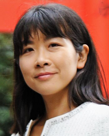
Marina Yamaguchi
KIOXIA CorporationMarina Yamaguchi was born in Hokkaido, Japan, in 1989. She received the B.S. (2012) and the M.S. (2014) in electrical and electronic engineering from Tokyo University of Agriculture and Technology, Tokyo, Japan. In 2014, she joined the Advanced LSI Technology Laboratory, the Corporate Research & Development Center, Toshiba Corporation, Japan, where she started her work on the research and development of emerging memory device technologies. She is currently with Kioxia Corporation (formerly Toshiba Memory Corporation) and has been assigned at Interuniversity Microelectronics Centre (IMEC), Leuven, Belgium as a device researcher, since 2021. Her main activities have been related to the electrical and reliability characterization of emerging memories including ferroelectric memory devices and materials. She is a member of JSAP.
-

Austin Lee Hickman
Cornell UniversityAustin Hickman is co-founder and CEO of Soctera, Inc., and holds a postdoc position in Electrical and Computer Engineering at Cornell University, working with Debdeep Jena and Grace Xing. His company and research focus on the fabrication and characterization of AlN-platform RF amplifiers.
Austin earned his Ph.D. from Cornell in 2021, and B.S. in Electrical Engineer-ing from the University of Notre Dame in 2016. He has authored over 10 jour-nal articles, over 10 conference presentations and 2 patents. Austin was born and raised in Huntington, West Virginia. He enjoys rowing with the Cornell Rowing Club and golfing with friends and family.
-
Quentin Wilmart
Univ. Grenoble Alpes, CEA, LETIQuentin Wilmart received the M.Eng. and the M.Sc degrees from the Ecole Supérieure de Physique et de Chimie Industrielles (ESPCI), Paris, France, in 2012. He received the Ph.D. degree in physics from the Ecole Normale Supérieure (ENS), Paris, France in 2015. He joined CEA-Leti in 2016, working on the design, fabrication and characterization of silicon photonic integrated circuits. His current research interests include the use of silicon nitride and IIIV materials for high-speed optical communication and quantum photonics. He is an author or co-author of more than 30 scientific papers and holds several patents.
-
Mikie Tsuji
University of TsukubaI was born in Tokyo in 1996.
I graduated from Koen Girls' School High School in 2015.
I entered the University of Tsukuba in 2015.
I received the B.E. and M.E. degrees of semiconductor engineering from University of Tsukuba under the guidance of Associate Professor Kaoru Toko, in 2019 and 2021, respectively.
I had been engaged in research on the synthesis of SiGe thin films by layer exchange and demonstrated SiGe thermoelectric generator on plastic substrate for the first time.
After completing the M.E. program, I joined Hitachi, Ltd. in 2021 and have been engaged in research and development of railway vehicles.
-
Taro Sasaki
The University of TokyoTaro Sasaki was born in Yamagata, Japan, in 1992. He received the B.E. and M.E degrees of electrical engineering from Tohoku University, Sendai, Japan in 2015 and 2017, respectively. He is currently pursuing the Ph.D. degree in material science at The University of Tokyo, Tokyo, Japan. His research interest includes 2D materials based electronic devices, especially 2D hetero-stack based non-volatile memory devices.
-
Shutaro Karube
Tohoku universityShutaro Karube has received Ph. D degree in Science from University of Tokyo, Japan in 2017. His Ph. D dissertation is regarding interconversion phenomena between spin and charge currents at metal/oxide interfaces via Rashba-Edelstein effect. This work has been mainly published in Applied Physics Express organized by IOP science and selected as an excellent paper award in Japan Society of Applied Physics in 2017. After the Ph. D, he has joined Tohoku university as an assistant professor and now is working on collinear antiferromagnetic oxide for exotic spin-orbit torque generation depending on Néel vector direction. This study has been reported by an oral presentation on SSDM2020 and selected as Young Researcher Award on the conference.
-
Takuya Wadatsumi
Kobe UniversityTakuya Wadatsumi received the B.S. and M.S. degrees in engineering from Kobe University, Kobe, Japan, in 2019 and 2021, respectively, where he is currently pursuing the Ph.D. degree in the fields of hardware security and Electromagnetic compatibility.
Call for 2021 SSDM Award Nomination
The SSDM Award was established to recognize outstanding contributions to academic or industrial development in the field of solid state devices and materials.
Papers to be nominated for the 2021 SSDM Award should be among those that have been presented between the 1st SSD conference in 1969 and the 47th SSDM conference in 2015.
The SSDM Award will ultimately be decided by the SSDM Organizing Committee after a recommendation is made by the SSDM Award Nomination Committee.
The recommendation will be in accordance with the following two criteria.
-
1) Originality
The award-winning selection must be original, and must have had significant theoretical or practical impact in the field of solid state devices and materials.
-
2) Contribution
The author(s) of the award-winning selection must have played or be playing a pioneering or leading role, with globally outstanding contributions in the technological field.
Candidate and Nominator Eligibility
-
- Candidates Eligible for the Award
All authors who presented papers between the 1st SSD conference in 1969 and the 47th SSDM conference in 2015, excluding papers written by this year’s Organizing Committee Chair and Award Nomination Committee Chair.
-
- Persons Eligible for Nominating Candidates
Anyone, excluding this year’s members of the SSDM Award Nomination Committee
Submission Process for SSDM Award Nominations
The following is the process for submitting nominations.
- - Before deciding on a candidate for the award, confirm the eligibility of nominators and candidates once again.
- - Download the Nomination Form.
SSDM Award Nomination Form [MS-Word] - - Fill out the Nomination Form and send it to the SSDM Secretariat by the nomination deadline.
The deadline for nomination has been extended till May 28, 2021. CLOSED
If you have any questions, please ask the secretariat by e-mail.
Sumitomo-shoji Kanda-Izumi-cho Bldg., 12F,
1-13 Kanda-Izumi-cho Chiyoda-ku Tokyo, Japan 101-0024
PAGE CONTENTS
closed.