

Awards
There are three categories of awards for authors who presented distinguished papers at SSDM.
SSDM Award
The SSDM Award is awarded to authors who contributed an outstanding paper at past SSDM.
A Low-Voltage Alterable Metal-Oxide-Nitride-Oxide-Semiconductor Memory with Nano-Meter Thick Gate Insulators (NM-MONOS)
This paper proposed the first MONOS nonvolatile semiconductor device and demonstrated its outstanding properties. The proposed structure reduced program voltage and increased speed and realized a memory device offering outstanding reliability, which opened the way for multi-layered flash memory in recent years. This structure is a core technology of 3D NAND memory, today's dominant storage memory, and supports larger capacities.
Nonvolatile memory using MOSFET was devised soon after MOSFET was developed in the 1960s. It is the main device supporting today's semiconductor industry. While floating-gate and charge-trapping mechanisms both originated at about the same time, they have been miniaturized and highly integrated in applications for different purposes. This paper focuses on a charge-trapping device that uses tunneling to a charge trap particular in the silicon nitride film to inject and hold the electron charge. Because the charge trap held the charge, the device, in principle, did not leak charge due to degradation of the insulating film in contrast to the floating-gate type, making it very reliable. Nevertheless, issues were faced in the significant property dispersion due to the use of traps scattered in the film as well as the difficulty of ascertaining device characteristics due to injected charge being discretely held in the nitride film. This paper proposed an additional ultrathin silicon oxide layer on top of the electron trap film. It became clear that this simple improvement greatly reduced the required amount of injected charge by keeping the charge trap away from the gate electrode, and this had profound effect on improving programming characteristics and retention characteristics.
Ever since the advent of NAND Flash memory, the floating gate had driven miniaturization, sweeping the market for large-capacity memory due to the simplicity of its memory operation and structure. However, around 2010, planar miniaturization, which had supported greater and greater capacities, reached its limit and 3D integration was needed. It was then that the MONOS memory device technology that this paper proposed once again came to the forefront on account of the advantage it offered of forming memory just by depositing insulator films, thereby paving the way for the creation of 3D nonvolatile memory.
For these reasons, this paper led to the realization of large-capacity storage memory, the core of today's semiconductor industry, and made a tremendous contribution to academic knowledge as well. This SSDM Award is presented in honor of those achievements.
-

Eiichi Suzuki
(ex) National Institute of Advanced Science and Technology (AIST)Eiichi Suzuki received the M.S., and Ph.D. degrees in Electronic Engineering from the University of Tokyo, Tokyo, Japan in 1972 and 1983, respectively. In 1972, he joined the Electrotechnical Laboratory (ETL), Ibaraki, Japan, where he was engaged in research and development of nonvolatile semiconductor memories, solar cells, quantum functional devices, and short-channel MOS devices. From 1985 to 1986, he was a Visiting Faculty Associate with the Department of Electrical Engineering, Arizona State University, Tempe, USA and worked on the characterization of a nonvolatile semiconductor memory. In April 2001, he joined the Nanoelectronics Research Institute (NeRI), National Institute of Advanced Industrial Science and Technology (AIST), Tsukuba, Japan, with the reorganization of ETL, and assumed the deputy Director of NeRI. Dr.Suzuki received the Ohm Technology Award in 1996. He is a fellow of the Japan Society of Applied Physics, and a member of the Institute of Electronics, Information and Communication Engineers of Japan.
-

Yutaka Hayashi
(ex) Toyota Technological Institute (contract temporally expired)Dr. Yutaka Hayashi joined Electrotechnical Laboratory (ETL) in 1964. There, he developed various early phase semiconductor devices; a tunnel source MOS transistor in 1965, Schottky TTL from 1967, VMOS and DMOS in 1969, 1 nsec DSA-ED logic in 1970, CHE injection FG memories from 1971.
In 1971-72, at Stanford University he worked on ultrasonic blood flow meters and developed silicon through-hole substrate technology for 3D integration.
On return to ETL, he joined "Sun-Shine Project" serving NEDO committees on solar cells up to 1992 and developed advanced solar cell technologies, e.g. thin (tens of µm) cSi solar cells, hetero junction cSi solar cells, etc. Meanwhile, in 1980~1992, he initiated the development of an early phase finFET, nanosheet FETs and MONOS memory as the future scaling-durable devices.
In 1992, he joined Sony Corp. and supervised the development of 0.25 to 0.18 µm MOSLSI technologies as the director of ULSI Research Laboratory, then served as a vice-president (for R&D) of Sony Semiconductor Company up to 1998.
After joining in an US venture (Halo LSI) in 1999, he was invited by AIST, Tsukuba in 2004 as an invited senior research fellow and developed new nano devices (e.g. columnar nano-memory: USP2010/0208522), until 2015.
He had been also a part time lecturer and then a project advisor of University of Tsukuba from 1981 to 2015 and an invited researcher of Osaka University from 2010 to 2017. He has been an invited fellow of Toyota Technological Institute from 2012 to 2023. -

Kenichi Ishii
(ex) Nanoelectronics Research Institute of AISTKenichi Ishii joined Electrotechnical Laboratory (ETL, later National Institute of AIST) in 1964.
He engaged in the development of basic processing technologies for silicon devices including CVD technologies for SiNx and Si thin films, and sold phase lateral epitaxy for thin bodies of early phase nanosheet FETs. Further, he worked for photolithography technologies up to excimer laser stepper technology. During the above technological development, he had made technical contributions in the development of various new MOS devices; finFETs, MONOS memories and nanosheet FETs in ETL and in AIST.
He passed away in 2009 while travelling in Hokkaido, Japan. -
Hisato Hiraishi
(ex) Citizen Watch Co.,Ltd.Hisato Hiraishi received Ph.D. degree in physical chemistry from the University of Tokyo in 1979. Since 1979 he worked for Citizen Watch and in 1980, sent by Citizen, joined the R&D group of the MONOS memory in the Electrotechnical Laboratory. In 1981 he returned Citizen and had been engaged in development of liquid crystal display, inkjet printer and new technologies for watch at the Technical Laboratory of the company. In 2000 he assumed the head of the Laboratory and then became a director of Citizen in 2003. After 2007 he took his position at two subsidiary companies; a managing director of Citizen Electronics and the president &CEO of Citizen Systems.
SSDM Paper Award (PA)
SSDM Paper Award is awarded to the best paper presented at the last SSDM.
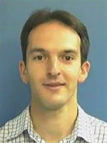
Impact of Back-side Power Delivery Network Layout on the FinFET Device Performance
-
Goutham Arutchelvan
imecGoutham Arutchelvan obtained his Master's degree in Microelectronics Engineering from TU Delft, Netherlands, in 2014. He completed his PhD in Materials Science at KU Leuven in 2021, where he collaborated with imec to research contacts to semiconducting transition metal dichalcogenides. Between 2019 and 2022, Goutham worked as a researcher at imec, concentrating on Si-based CMOS and beyond CMOS devices. He was involved in exploring backside power delivery for Si-FinFET technologies and modeling thin film transistors like IGZO for back-end functionality. Goutham has co-authored 40 papers and has been a reviewer for numerous journals, such as Nature Nanotechnology, ACS Electronic Materials, Applied Physics Letters, IEEE Transactions on Electron Devices. Currently, he works as the Principal Engineer at TSMC's Corporate Research in Taiwan, where he is interested in exploring new channel materials for front-end and back-end logic.
-
Thomas Chiarella
imecT. Chiarella received the M. Sc. Degree in Electronics from the "Institut Supérieur Industriel Catholique du Hainaut" in Charleroi, Belgium in 2002. He directly joined the Silicon Process & Device Technology division of imec as Characterization Engineer and took part, as Device Engineer, in technology transfers (130nm, 90nm, 65nm, 14nm) and the baseline yield improvement. He takes part in imec's Affiliation Program focusing on successful and efficient definition and evaluation of finFET, nanosheet and CFET technologies. He is now Senior Researcher in charge of finFET and CFET device design. He has actively contributed to the Horizon 2020 ASCENT EU project (Project no. 654384). In addition to own publications in ICMTS/ESSDERC proceedings and Solid-State Electronics journal, he contributed to more than 50 technical papers (mainly IEDM/VLSI).
-
Hiroaki Arimura
imecHiroaki Arimura is a principal member of technical staff at imec, Belgium. He received M.S. and Ph.D. degrees in engineering from Osaka University, Japan, in 2009 and 2011, respectively. In 2011, he joined imec, Belgium, as a postdoctoral researcher and studied NBTI reliability of ultra-thin EOT devices. He became a researcher of imec in 2013 and engaged in a development of metal / high-k gate stack on high-mobility channel materials such as Ge and SiGe, and conducted device studies including FinFET and Gate-All-Around nanowire transistors. Currently, he is leading the gate stack module development for advanced logic and memory peripheral devices.
-
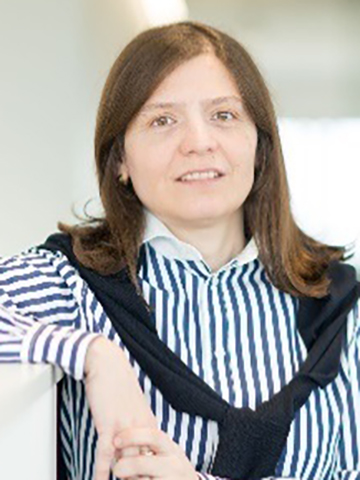
Anabela Veloso
imecAnabela Veloso received a Ph.D. from INESC-IST-Lisbon University, Portugal in 2002. Since 2001, she has been working at Imec, in Leuven, Belgium, where she is a principal member of technical staff. Currently, her main research interests are in the areas of advanced CMOS device physics, integration, characterization, and technology, with recent focus on the exploration of scaled nanowires/nanosheets based FETs (with lateral or vertical transport), logic with functional backside, buried power rails, nTSVs, and overall novel device schemes while also taking into consideration possible new options for transistor engineering and connectivity from the wafer’s front/backside. She has authored or co-authored more than 200 papers published in peer-reviewed international conference proceedings and technical journals, presented 20 invited conference talks, and has been (co-)inventor of more than 23 filed/granted patents. She has also been serving in several conference committees including IEDM, SSDM, ECS Meeting, and the Symposium on VLSI Technology and Circuits.
-

Anne Jourdain
imecAnne Jourdain received her PhD degree in Physics from University Joseph Fourier of Grenoble, France, in 1998. In 1999, she joined IMEC (Interuniversity Microelectronics Center) in Leuven, Belgium, to work on wafer-level-packaging solutions for RF-MEMS applications. In 2007, she joined the 3D Integration Research Program of IMEC to work on various wafer-to-wafer bonding and wafer thinning technologies. In 2019, she became responsible for the Backside Power Delivery Network integration activities within the program before taking the lead of the 3D Heterogeneous Integration team in 2022, looking at collective die-to-wafer and direct hybrid bonding technologies for 3D stacking applications.
-
Eugenio Dentoni Litta
imec -

Naoto Horiguchi
imecNaoto Horiguchi is the director of CMOS device program in imec, Leuven, Belgium. He started his carrier in semiconductor device R&D in Fujitsu Laboratories Ltd. in 1992. In 1992-1999, he was engaged in device R&D by using semiconductor nano structures in Fujitsu laboratories Ltd. and University of California, Santa Barbara. In 2000-2006, he was engaged in 90-45nm CMOS technology development in Fujitsu Ltd. From 2006, he is with imec, Leuven, Belgium, where he is engaged in advanced CMOS device R&D together with worldwide industrial partners, universities, and research institutes. His current focus is CMOS device scaling for 10Å technology node and beyond.
-
Jérôme Mitard
imecJérôme Mitard received the Ph.D. degree in microelectronic engineering from the Polytechnic University School of Marseille (France), in 2003. Over three years, he acted as an STMicroelectronics assignee with CEA-LETI, Grenoble, France, where he was deeply involved in the electrical characterization and reliability of hafnium-based dielectric stacks with replacement metal gate targeting sub-45nm node complementary metal–oxide–semiconductor (CMOS) logic technologies. After his Ph.D. in microelectronics at INPG, France, he joined the R&D center IMEC, Leuven, Belgium, as a device researcher, working on the experimental demonstration of the germanium-based high-mobility channels in planar, Fin and GAA FET architectures. He also technically led the development of the IGZO-based transistors fueling the active BEOL and DRAM roadmaps. In parallel, he joined the staff management team, first as a team leader of the compute device research and now expanding his leadership role toward quantum devices as a R&D device manager in imec.
SSDM Best Student Award (BSA)
SSDM Best Student Award is awarded to the best student paper presented at the last SSDM. This award was established from SSDM 2022.
Mobility Enhancement in Extremely-Thin Body (110) SiGe-on-insulator pMOSFETs using Starting Substrates with Thin SiGe Layers
-
Chia-Tsong Chen
The University of TokyoChia-Tsong Chen received the B.E. and M.E. degree in electronics engineering from the National Chiao Tung University, Hsinchu, Taiwan in 2016 and 2019 respectively. He received Ph.D. degree in the Department of Electrical Engineering and Information Systems, School of Engineering from the University of Tokyo in 2022 under the supervision of Prof. Shinichi Takagi. After his Ph.D., he joined the University of Tokyo as a post-doctoral researcher with the aim to investigate the impact of performance enhancement through strain engineering in extremely-thin body (Si)Ge channels. Since April 2023, he has been working as a researcher in Device Technology Research Institute in National Institute of Advanced Industrial Science and Technology (AIST) for advanced device process research. His research interest includes the advanced technology and innovations for future CMOS devices, such as high mobility material for extremely-thin body channel, 3D heterogeneous integration, and ferroelectric HfO2-based materials for gate stack and memory applications.
SSDM Young Researcher Award (YRA)
SSDM Young Researcher Award is awarded to the first authors who presented excellent papers at the last SSDM. The author should be 33 years old or younger as of April 1st in the next year of the conference. Recipients of the PA and BSA are not eligible for the YRA.
Tumor-on-a chip in 3D microfluidic device for immunotherapy study
-
Yu-Chen Chen
National Tsing Hua UniversityYu-Chen Chen get her Ph.D degree in Power Mechanical Engineering Department from National Tsing Hua University, Taiwan. She joined the Micro-Systems and Control Lab in 2018. Her research includes Lab on Chip, Organ on Chip, digital microfluidic systems and Nanotechnology used in cancer research and drug screening. She received awards from FUTEX (2021), 18th National Innoaward, and 2022 the best paper award at the thesis presentation competition, college of engineering, National Tsing Hua University.
A High-Efficiency, Reliable Multilevel Hardware-Accelerated Annealer with In-Memory Spin Coupling and Complementary Read Algorithm
-

Yun-Yuan Wang
Macronix International Co., Ltd.Yun-Yuan Wang earned a Bachelor of Science in Physics from National Tsing Hua University (NTHU) and a Master of Science in Photonics and Optoelectronics from National Taiwan University (NTU) in 2019. Now, he serves as a Principal Research Engineer at the Emerging Central Laboratory in Macronix International, where he has gained extensive cross-disciplinary research experience in fields ranging from deep learning to advanced memory, semiconductor devices, and quantum computing.
Throughout his 3-year career at Macronix, Yun-Yuan has published 5 papers in international journals and top conferences. He also holds a total of 13 licensed patents in-memory computing, quantum-inspired algorithms, and two-dimensional materials.
Group IV Semiconductor Alloy Thin Films for Environmentally Friendly
-
Shintaro Maeda
University of TsukubaShintaro Maeda was born in Nagasaki, Japan, in 1999.
He received the B.E. degree of semiconductor engineering from University of Tsukuba under the supervision of Associate Professor Kaoru Toko, in 2022. He is presently a second-year student in the master's program.
He focuses on group IV semiconductor materials (germanium, silicon and tin). In particular, his research involves low-temperature and high-quality synthesis of the alloy thin films and their device applications, including thermoelectric conversion devices.
After completing the M.E. program, he plans to go on to a Ph.D. program where he will work on thin-film solar cell and transistor applications as well as thermoelectric applications of group IV alloy semiconductors.
Neural Network Hardware Accelerator using Memristive Crossbar Array based on Wafer-Scale 2D HfSe2
-
Sifan Li
National University of SingaporeSifan Li is currently a research fellow in National University of Singapore (NUS), Singapore. He obtained his Ph.D. degree from the Department of Electrical and Computer Engineering at NUS in 2022. His research interests focus on the development of advanced memory technologies based on two-dimensional (2D) materials for neuromorphic/in-memory computing applications to overcome the energy and latency limitations of traditional von-Neumann computing system. Specifically, he works on the design, fabrication, and characterization of 2D materials-based memristors and crossbar arrays for implementing neural network hardware accelerator. His research contributes to pathways for addressing challenges associated with memristor-based computing architecture, including the energy consumption and variability of memristors, the scalability of 2D materials growth, and unveiling the operating mechanism in novel 2D materials-based resistive switching (RS) medium. Currently, he is working on heterogeneous integration of 2D/Si for large-scale memristive crossbar array and its hardware implementation of compute-in-memory system.
Electro-optic imaging system using a CMOS image sensor with a dual-layer on-pixel polarizer
-
Ryoma Okada
Nara Institute of Science and TechnologyOkada was born in Aichi, Japan, in 1997. He received his B.E. degree in electrical and electronic engineering from Shizuoka University, Shizuoka, Japan, in 2020, and his M.E. degree in the Division of Materials Science from the Nara Institute of Science and Technology (NAIST), Nara, Japan, in 2022. His affiliation is the doctoral course student of Photonic Device Science Laboratory with the NAIST and a cooperative visiting researcher of Radio Research Institute, the National Institute of Information and Communications Technology, Tokyo, Japan. His current research interests involve polarization image sensors for detecting weak polarization changes, and high-frequency electromagnetic field imaging based on electro-optic effects.
Vertical Alignment Control of Self-Ordered Multilayered Ge Nanodots on SiGe
-
Wei-Chen Wen
IHP - Leibniz Institute for High Performance MicroelectronicsWei-Chen Wen received her Master's and Ph.D. degrees in engineering from Kyushu University, Japan, in 2017 and 2020, respectively. Her research was defect characterization of Ge gate stacks using deep-level transient spectroscopy. She joined IHP GmbH - Innovations for High Performance Microelectronics in 2021. She is working on Group IV epitaxy, including 3D self-aligned nanodot growth, lateral selective growth of defect-free virtual substrate and other applications in quantum devices and heterojunction bipolar transistors.
Polarization-Independent Enhancement of Optical Absorption in a GaAs Quantum Well Embedded in an Air-bridge Bull's-eye Cavity
-
Sangmin Ji
The University of TokyoBorn in 1990.01.06.
Bachelor
Hiroshima University (2009.04–2013.03).
Master
The University of Tokyo (2013.04–2015.03).
Doctor
The University of Tokyo (2019.04–2022.09).
Working experience
Research Engineer, EO Technics (2015.04–2016.11).
Senior Research Engineer, LG Electronics (2016.11–2019.02).
Project Researcher, Institute of Industrial Science, The University of Tokyo (2022.10–2022.03).
Project Research Associate, Institute of Industrial Science, The University of Tokyo (2023.04–Present).
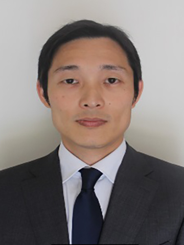
Presentation No. E-3-06 [Area 10]Utilizing Dual-stacked IGZO channel structure to Achieve Optical Memories Application
Kuan-Ju ZhouNational Sun Yat-Sen University, Taiwan-

Kuan-Ju Zhou
National Sun Yat-Sen UniversityKuan-Ju Zhou is currently pursuing his Ph.D. degree with the Department of Physics, National Sun Yat-Sen University (NSYSU), Taiwan. His current research topics include resistive random-access memory (RRAM), amorphous silicon thin film transistors (TFTs), low temperature polysilicon TFTs, metal oxide semiconductors TFTs, and GaN High Electron Mobility Transistor with emphasis on the device physics, reliability issues, device simulation, and process integrations. He received his B.S. degree from the Department of Physics, National Sun Yat-Sen University (NSYSU), Taiwan, in 2018. He continued his master degree in the Department of Physics, NSYSU at 2018, and then started his Ph.D. career at 2019. In the fourth year of his Ph.D. (2022~2023), he was a Visiting Fellow at the Tokyo Institute of Technology, Laboratory for Materials and Structures, under the supervision of Prof. Toshio Kamiya and Prof. Keisuke Ide. He was working on TCAD simulation, parameter extractions, and machine learning for amorphous oxide semiconductors.
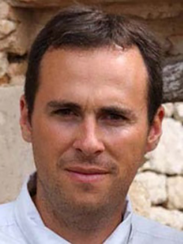
Presentation No. C-10-06 [Area 9]Highly Efficient Spin Current Source Using BiSb Topological Insulator / NiO Bilayers
Julian SasakiTokyo Institute of Technology, Japan-
Julian Sasaki
Tokyo Institute of TechnologyJulian Sasaki received his master's degree in Tokyo institute of technology under the guidance of professor Pham Nam Hai. Research interests were to investigate the possibilities for a more practical use and manufacturing process for devices utilizing topological insulator, BiSb. Studies ranged from optimizing SOT-MRAM memory structure using BiSb to researching the possibility of using the inverse spin Hall effect for magnetic field sensors. Studies including the findings from the presentation given in SSDM 2022, were awarded the excellent Master's thesis award in march 2022. Julian Sasaki currently works in Tokyo Electron Ltd. as a process engineer for diverse systems and solution device researches.
-
Call for 2023 SSDM Award Nomination
The SSDM Award was established to recognize outstanding
contributions to academic or industrial development in the field
of solid state devices and materials.
Papers to be nominated for the 2023 SSDM Award should be among those
that have been presented between the 1st SSDM conference in 1969
and the 49th SSDM conference in 2017.
The SSDM Award will ultimately be decided by the SSDM Organizing Committee after a recommendation is made by the SSDM Award Nomination Committee.
The recommendation will be in accordance with the following two criteria.
-
1) Originality
The award winning selection must be original, and must have had significant theoretical or practical impact in the field of solid state devices and materials.
-
2) Contribution
The author(s) of the award-winning selection must have played or be playing a pioneering or leading role, with globally outstanding contributions in the technological field.
Candidate and Nominator Eligibility
-
–
Candidates Eligible for the Award
All authors who presented papers between the 1st SSD conference in 1969 and the 49th SSDM conference in 2017, excluding papers written by this year's Organizing Committee Chair and Award Nomination Committee Chair.
-
–
Persons Eligible for Nominating Candidates
Anyone, excluding this year's members of the SSDM Award Nomination Committee
Submission Process for SSDM Award Nominations
The following is the process for submitting nominations.
- – Before deciding on a candidate for the award, confirm the eligibility of nominators and candidates once again.
-
– Download the Nomination Form.
[ SSDM Award Nomination Form (MS‐Word) ] -
– Fill out the Nomination Form
and send it to the SSDM Secretariat by the nomination
deadline.
Nomination deadline: May 15, 2023 CLOSED
If you have any questions, please ask the secretariat by e‐mail
Sumitomo‐shoji Kanda‐Izumi‐cho Bldg., 12F,
1‐13 Kanda‐Izumi‐cho Chiyoda‐ku Tokyo, Japan 101‐0024