|
|
 |
AWARDS
History of SSDM Award
For the history of SSDM Award please click here.
SSDM Award 2013
SSDM 2013 presents the SSDM Award to two outstanding papers; Hidetake Suzuki, Katsuhiko Suyama, Koichiro Odani, Masumi Fukuta former employees of Fujitsu Laboratories Ltd., for the presentation of the paper entitled "C-band 10W Power GaAs MESFET with an Internal Matching Circuit" and Yohichi Aono, Asamitsu Higashisaka, Tadayuki Ogawa, Fumio Hasegawa former employees of Central Research Laboratories, Nippon Electric Co. Ltd., for the presentation of the paper entitled "X- and Ku-band Performance of Submicron Gate GaAs Power FETs" both presented at the 9th International Conference on Solid State Devices (1977), Tokyo
"C-band 10W Power GaAs MESFET with an Internal Matching Circuit"
Fujitsu Laboratories Ltd.
"X- and Ku-band Performance of Submicron Gate GaAs Power FETs"
Central Research Laboratories, Nippon Electric Co. Ltd.,
presented at the 9th International Conference on Solid State Devices (1977), Tokyo.
The above two papers describe the "development of high-power GaAs FETs" that were successively presented at 1977 SSDM. The former, by Fujitsu, is on the C-band (4 to 8 GHz) and the latter, by NEC, is on the X-band (8 to 12 GHz) and Ku-band (12 to 18 GHz).
It is widely known that expanding the gate width of an FET increases the output power and reducing the gate length extends the frequency range. However, the wider the gate, the lower the input impedance becomes, which results in impedance mismatch. And reducing the gate length increases the transmission loss along the gate width. The above two papers provided ideas for resolving these problems. The Fujitsu paper suggests and examines dividing an FET into many parts and letting them operate in parallel (unit gate length: 1.5 µm; total gate width: 15,000 µm), and realizes internal matching with MOS capacitance and bonding wire inductance. Fujitsu succeeded in an output exceeding 10 W in the C-band (4 GHz) at a drain voltage of 18 V, which was the first in the world and an epoch-making achievement.
To extend frequency ranges to the X- and K-bands, it is necessary to reduce gate length. The above paper by NEC reported success in achieving high output in the X- and Ku-bands by applying reduced gate length (0.5 µm) technology that had been developed or low-noise FETs at the NEC to large gate width FETs. Ten FETs with a gate width of 75 µm were connected in parallel to form a unit, and two to four such units operated in parallel (with a total gate width of 3,000 µm). In this way, group succeeded in reaching 0.65 W in the Ku-band (13.6 GHz) and 1 W in the X-band (11 GHz).
Regarding the development of GaAs Power FETs, the Fujitsu research group was three to four years ahead of the rest of the world. After starting research around 1973 Dr. Fukuta of Fujitsu Laboratories Limited gave an invited lecture on GaAs power FETs at the 1975 SSDM and commercial production commenced in 1976. During this time, NEC as well as other world-wide companies began full development. Since then, fierce competition has taken place to increase output power and extend frequency ranges. Researchers all over the world pursued improvement in the basic characteristics of GaAs FETs (lower noise, higher efficiency, greater linearity, HEMT structure, high breakdown voltage recess structure, internal impedance matching, dual-gate, Doherty circuit, etc.). Against this backdrop, the above two papers represented landmarks in the development of high-power GaAs FETs, 10 W in the C band and 1 W in the X- and Ku-bands. The research also ushered in development of the market for high-power GaAs FETs. It can be said that these papers broke new ground in developing the market not only for GaAs FETs but also for extremely high power compound semiconductor FETs such as GaN HEMTs with an output reaching 1,000 W.
In this context, the papers are pioneering works in the development of high power GaAs FETs for microwave applications.
"C-band 10W Power GaAs MESFET with an Internal Matching Circuit"
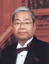
Hidetake Suzuki
Hidetake Suzuki was born in Shizuoka, Japan, on July 31, 1945. He received the B.S. and M.S. degrees in applied physics from Tokyo University of Science, Japan, in 1969 and 1971, respectively. In 1974 he joined the Semiconductor Laboratory, Fujitsu Laboratories Ltd., Kawasaki, Japan, where he was engaged in the research and development of power GaAs MESFETs until 1990. In 1990, he moved to Fujitsu Yamanashi Electronics in Kohfu where he worked for mass-production of GaAs power FETs. Mr. Suzuki was a member of the Japan Society of Applied Physics and the Institute of Electronics and Communication Engineering of Japan. |
 |
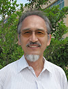
Katsuhiko Suyama
Katsuhiko Suyama received the B.E. and M.E. degrees in electrical engineering from Keio University in 1970 and 1972, respectively. In 1972, he joined the Semiconductor Laboratory, Fujitsu Ltd. where he was concerned with the design and characterization of GaAs low-noise and power MESFET’s and GaAs digital integrated circuits. In 1982, he was transferred to the factory and organized the project team to develop GaAs ICs for telecom and computer application and bore fruit as the Fujitsu VPP500 commercial supper computer in 1992. In 1995-1997, he was the manager of international procurement office at Fujitsu Microelectronics Asia Pte.Ltd. in Singapore. In 2000, he left Fujitsu and applied to Japan International Cooperation Agency (JICA) for senior volunteer. He taught electronics at vocational training center and/or technical college in Kathmandu, Nepal 2001-2003, in Kulim, Malaysia 2004-2006 and in Phnom Penh, Cambodia 2009-2011. Currently, he is the chairman of NPO Senior Overseas Volunteer Associates. |
 |
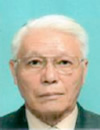
Koichiro Odani
Koichiro Odani was born in Osaka, Japan, on September 27, 1943. He graduated from the Tsu Institute of Technology, Mie, Japan, in 1963. In 1963, he joined Kobe Industries Company, later merged with Fujitsu Limited in 1973. From 1963 to 1973, he was engaged in developing Si RF power transistor and Si integrated circuit. From 1973 to 1993, he was engaged in developing high power GaAs FETs for satellite communication, low noise HEMTs for DBS receiver and HEMT LSIs for supercomputer applications as a Section Manager, Fujitsu Laboratories Ltd., Atsugi, Japan. From 1993 to 2000, he was engaged in manufacturing of GaAs IC products as a Manager, Fujitsu Quantum Devices Co., Ltd., Yamanashi. From 2000 to 2004, he was engaged in developing high power 3C-SiC vertical DMOSFETs for EV/HEV inverters as a General Manager, HOYA Corporation. Since 2012, he is currently a Director at Soubudai-Community Center, Sagamihara-city, Japan. |
 |
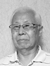
Masumi Fukuta
Masumi Fukuta received the B.E. degree from Nagoya Institute of Technology in 1963 and the Ph.D.degree in electrical engineering from Nagoya University in 1977. In 1963, he joined Kobe Industries Co. which later merged with Fujitsu Ltd. In 1967, he invented Mesh Emitter Transistor for RF power application. In 1971, he started development of GaAs power FET and from 1976 to 1980 supervised GaAsICs and HEMT project in Fujitsu Laboratories. In Fujitsu Ltd., he served as general manager of compound semiconductor div. and a director of Fujitsu Ltd. In 1997, he was appointed president of Fujitsu Quantum Devices Ltd. From 2004 to 2006, he performed as chairman & CEO of Eudya Devices Inc. In 1997, he received a prize medal from the Minister of Science and Technology in Japan for outstanding contributions in development of GaAs Power FETs. In 1988, he received Microwave Application Award from MTT society of IEEE for recognition and demonstration of the potential of GaAs FETs for power applications. |
 |
"X- and Ku-band Performance of Submicron Gate GaAs Power FETs"
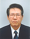
Yohichi Aono
Yohichi Aono was born in Ibaraki, Japan, on November 27, 1943. He graduated from Mito Technical High School, specializing in electrical engineering, in 1962. He joined Nippon Electric Company Ltd., Kawasaki, Japan in 1962, andworked on millimeter-wave electron tubes, Gunn diodes, and GaAs IMPATT diodes. He was engaged in the development of GaAs power FET's as a Member of the Technical Staff in the Central Research Laboratory, Nippon Electric Company until 1982. He was also engaged in the production of GaAs FET's until 1992 and, then, worked as an application engineer, retired in 2003. |
 |
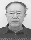
Asamitsu Higashisaka
Asamitsu Higashisaka received Master of Engineering degree from Hiroshima Univ. and joined NEC Corp. in 1969. In NEC he was engaged in the research and development of compound semiconductor devices including GaAs FETs, microwave ICs and digital ICs. He also managed optoelectric devices development such as laser diodes and photo detective diodes, as well as microwave devices development. In 2000, he transferred to Anritsu Corp., where he was promoted, as a chief engineer, forthe development of wide-band amplifiers and optoelectric components for optical communication system application. From 2004 to 2012, he lectured at Tokai University on optical communication system, radio application system and information communication engineering. He and his colleagues were awarded The Okochi Memorial Prize for the development of power GaAs FET in 1979. He received Doctor of Engineering degree from Tokyo Institution of Technology in 1982. |
 |
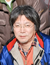
Tadayuki Ogawa
Tadayuki Ogawa joined Central Research Laboratories, Nippon Electric Company Ltd., Kawasaki, Japan in 1974. He was engaged in the research and development of compound semiconductor devices for microwave applications. In 1981, he moved to Electronic circuit component division, where he worked for the developments of micro-capacitors and –resistors of computers and communication circuit boards. In 1985, he moved to Sales division in NEC. After that, he served sales of electronic components and color liquid crystal display components. He retired in 2012. |
 |
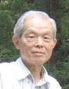
Fumio Hasegawa
Fumio Hasegawa received B.S., M.S., and Dr. of Engineering degrees in electronics engineering from Tohoku University, Sendai, Japan, in 1963, 1965 and 1973, respectively. In 1965 he joined Central Research Laboratories, Nippon Electric Company, Ltd., Kawasaki, Japan, where he worked on the development of GaAs vapor phase epitaxy, Gunn diode, GaAs IMPATT diodes, and GaAs MESFET’s. From 1974 to 1975, he was with The University of Sheffield, England, as a Senior Research Fellow. He moved to University of Tsukuba as an Associate Professor in 1981, promoted to a full Professor in 1988 and retired in 2004. He worked on deep levels in GaAs, HVPE growth of GaAs, AlGaAs and GaN, and MBE growth of Si and SiGe for infrared detector. From 2004 to 2008, he was a Professor of Kogakuin University, and gave lectures until 2011. Dr. Hasegawa was given a Professor Emeritus by University of Tsukuba in 2004. |
 |
HISTORY OF SSDM AWARD
|

